Table of Contents
Advertisement
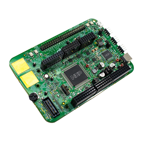
S32K148 Telematics Box
Reference Design Board
CONTENTS:
Get to know the S32K148 T-BOX Reference Design Board
(RDB)
S32K148 T-BOX RDB out-of-the-box setup
Creating a new S32DS project for the S32K1xx MCU
S32DS debugging basics
Create a P&E debug configuration
GET TO KNOW THE S32K148-T-BOX REFERENCE DESIGN BOARD (RBD)
Potentiometer
SW2 & SW3:
Touch Pad
J25&J27:
4G module
connector
Audio Codec:
STGL5000
P1:Mic input
SW4: User
bottom
J28: GPS
module
connector
SW5: User
bottom
J15:
TJA1101
MCU:
Line
S32K148
OUT
J16:
J15:
Audio
Line
OUT
OUT
Figure 1: S32K148-T-BOX Reference Design Board (RBD)
J26: BLE
module
J5: CAN0
connector
interface
RGB LED
SBC HVIO
SBC:
UJA113x
SW1: Reset
bottom
J31:23-pin
ECU connector
Route signals with:
• 3x CAN bus
• 2x LIN bus
• 1x Ethernet
• 2x Analog input
• 2x HS output
• 2x Input Capture
• 12 V Power Supply
Advertisement
Table of Contents

Related Manuals for NXP Semiconductors S32K148


Summary of Contents for NXP Semiconductors S32K148
- Page 1 S32K148 Telematics Box Reference Design Board CONTENTS: Get to know the S32K148 T-BOX Reference Design Board (RDB) S32K148 T-BOX RDB out-of-the-box setup Creating a new S32DS project for the S32K1xx MCU S32DS debugging basics Create a P&E debug configuration...
- Page 2 23-pin ECU connector and also expends 1 CAN and 2 LIN bus Select TJA1044 with SO-8 and TJA1043 S32K148 T-BOX_GP-ECU RDB WITH ALL MODULES PLUGIN with HVSON14 package to compatible with Stinger Use a 23-pin ECU connector to route...
- Page 3 Standby mode - Data sheet (REV 6) Audio Codec: SGTL5000 S32K148-T-BOX RBD SOFTWARE PACKAGE SGTL5000, Low Power Stereo Codec with The S32K148 T-BOX_GP-ECU RDB SW Headphone Amp - Data Sheet (REV 6.0) package is based on S32K SDK and 3-axi Accelerator: MMA8452Q is developed to accelerate customer’s...
- Page 4 PINOUT MAPPING OF ARDUINO™ UNO HEADER PORT PORT PORT J17-28 PTE15 J17-29 PTB12 J17-30 PTD31 J17-25 PTE16 J17-26 PTB13 J17-27 PTD26 J17-22 VREFH J17-23 PTE11 J17-24 PTD25 J17-19 J17-20 PTE10 J17-21 PTC26 J17-16 PTB2 J17-17 PTB11 J17-18 PTC25 J17-13 PTB3 J17-14 PTB17 J17-15 PTC24...
- Page 5 HEADER/PINOUT MAPPING FOR S32K148 External On-board Used MCU Function Pin S32K148 MCU Pins Modules Connector Peripherals UART-TX PTB0/LPUART0_RX J26-1 BLE module LPUART0 UART-RX PTB1/LPUART0_TX J26-2 UART-TX PTC8/LPUART1_RX J28-3 GPS module UART-RX PTC9/LPUART1_TX J28-2 LPUART1 PTC10/FTM3_CH4/TRGMUX_IN11 J28-1 UTXD1 PTD17/FTM0_FLT2/LPUART2_RX/FTM5_FLT1 J25-6 URXD1...
- Page 6 HEADER/PINOUT MAPPING FOR S32K148 CONT. External On-board Used MCU Function Pin S32K148 MCU Pins Modules Connector Peripherals SBC_SPI_CS PTA26/FTM5_CH1/LPSPI1_PCS0 SBC_SPI_SCLK PTA28/FTM5_CH3/LPSPI1_SCK/LPUART0_RX LPSPI1 SBC_SPI_MOSI PTA29/FTM5_CH4/LPUART2_TX/LPSPI1_SIN SBC_SPI_MISO PTA27/FTM5_CH2/LPSPI1_SOUT/LPUART0_TX SBC_CAN_TXD PTE5/TCLK2/FTM2_CH3/CAN0_TX/FXIO_D7 CAN0 SBC_CAN_RXD PTE4/TRACE_D1/FTM2_CH2/CAN0_RX/FXIO_D6 SBC_LIN1_TXD PTA3/LPUART0_TX/FXIO_D5 LPUART0/ FlexIO4_5 SBC_LIN1_RXD PTA2/LPUART0_RX/FXIO_D4 SBC(UJA113X) SBC_LIN2_TXD PTA9/LPUART2_TX/LPSPI...
- Page 7 CANL0 pink CAN bus 0 differential signal- below photo. black 1.25 Signal ground It is not included in S32K148 T-BOX 100M-base TX1 automotive ENET_TRX_P green ethernet differential signal+, RDB, please contact NXP sales for purchase: 100M-base TX1 automotive...
- Page 8 It’s connected between VDD and VDD_MCU, and is designed for 1-2 (Default) S32K148 MCU low-power static current measurement, for this case, R77 needs to be unmounted. The jumper connection schematic is as below, details can be found in the board schematic;...
- Page 9 USING ETHERNET AND QSPI IMPORTANT OBSERVATION S32K148 shared PIN Configuration resistor Description The S32K148 is the only member of the PTD7 R161 (Default) ENET: MII_RMII_TXD1 family able to use ethernet and QuadSPI. R162 QuadSPI: QSPI_A_IO1 However, these interfaces are mutually...
- Page 10 Out-of-the-Box Setup POWER UP THE BOARD AND S32K148 T-BOX RDB SETUP CONNECTION DEBUGGER CONNECTION The S32K148 T-BOX RDB powers from external +12V power supply via the USB Cable to PC 23-pin ECU connector with the wiring DC - 12 V harness.
- Page 11 Use the BSP test project STEP 1: DOWNLOAD & INSTALL S32DS FOR ARM V2018.R1 AND S32K SDK RTM 2.0.0 Download S32DS for ARM v2018.R1 from the following link: http://www.nxp.com/S32DS – The download will require a NXP account login, user can register the account with any e-mail, and after download, you can install S32DS IDE with a 32-bit active code received by the e-mail when download ...
- Page 12 STEP 2: IMPORT AND COMPILE THE BSP TEST PROJECT (2) Select archive file > Browse, browse and choose S32K148_Based_T_BOX_BSP_TestPrj_SDK_RTM2_0.zip, select the project > Finish: After importing the project, clean it at first: select the project in Project Explorer, then right-click, choose Clean Project:...
- Page 13 STEP 2: IMPORT AND COMPILE THE BSP TEST PROJECT (3) Select the project in Project Explorer, then right-click, choose Build Project: The compile result is as below if no errors are found:...
- Page 14 STEP 3: DOWNLOAD AND DEBUG THE BSP TEST PROJECT Select the project in Project Explorer, then right-click, choose Debug As > Debug Configuration: In the Debug Configuration window, select the GDB PEMicro Interface Debugging > S32K148_Based_T_BOX_BSP_TestPrj_ SDK_RTM2_0_Debug>Debugger>under Interface select right debugger, and ensure Port has the right part number, then in Additional Options, check Emergency Kinetis Device Recovery by Full Chip Erase and Use SWD protocol (if not check this option, it will use JTAG debug protocol), at last, click Debug to launch the debug(it will download the compile result—elf file in to the target MCU at first):...
- Page 15 STEP 4: CONNECT THE UART CONSOLE FOR TEST RESULT OUTPUT DISPLAY The BSP test project use S32K148 LPUART2 to output the test result; Use a USB-to-UART adapter to connect the board with PC via J25-6(TXD), J25-7(RXD) and J25-12(GND): * For more details on the test results description and demo projects, please refer to the Software User Guide.
- Page 16 – LIN stack based Single board LIN master and slave communication demo project – I S audio codec—SGTL500 demo project – T-BOX reference design project * For more details, please refer to the S32K148 T-BOX_GP-ECU RDB SW user guide and download the SW package...
- Page 17 Create a New Project in S32 Design Studio CREATE NEW PROJECT: FIRST TIME – SELECT A WORKSPACE Start program: Click on “S32 Design Studio for ARM v1.0” icon Select workspace: – Choose default (see below example) or specify new one –...
- Page 18 CREATE NEW PROJECT: S32DS PROJECT Project Name: – Example: FirstProject Project Type: – Select from inside executable or library folder Next Select Debugger Support and Library Support Click Finish...
- Page 19 OPENSDA CONFIGURATION To Debug your project with OpenSDA, it is necessary to select the OpenSDA in the Debug Configuration. Select your project, and click on debug configuration Select the Debug configuration under GDB PEMicro Interface Debugging Click on Debugger tab ...
- Page 20 Debug Basics DEBUG BASICS: STARTING THE DEBUGGER Debug configuration is only required once. Subsequent starting of debugger does not require those steps. Three options to start debugger: – If the “Debug Configuration” has not been closed, click on “Debug” button on bottom right –...
- Page 21 DEBUG BASICS: VIEW & ALTER VARIABLES View variables in “Variables” tab. Click on a value to allow typing in a different value. DEBUG BASICS: VIEW AND ALTER REGISTERS View CPU registers in the “Registers” tab Click on a value to allow typing in a different value ...
- Page 22 DEBUG BASICS: BREAKPOINTS Add Breakpoint: Point and Click Light blue dot represents debugger breakpoint DEBUG BASICS: RESET & TERMINATE DEBUG SESSION Reset program counter Terminate Ctl+F2()
- Page 23 Create a P&E Debug Configuration (Optional) NEW P&E DEBUG CONFIGURATION Click in debug configurations Create a new P&E launch configuration Select S32K144 device Click Apply and debug your application...
- Page 24 NXP and the NXP logo are trademarks of NXP B.V. All other product or service names are the property of their respective owners. © 2019 NXP B.V. Document Number: S32K148TBOXEFS REV 0...
Need help?
Do you have a question about the S32K148 and is the answer not in the manual?
Questions and answers