Table of Contents
Advertisement
Quick Links
NXP Semiconductors
User Guide
S32R274/372 EVB User Guide
by : NXP Semiconductors
1. Introduction
This user guide details the setup and configuration of the
NXP S32R274/372 Evaluation Board (hereafter referred
to as the EVB). The EVB is intended to provide a
mechanism for easy customer evaluation of the S32Rxx
family of microprocessors, and to facilitate hardware and
software development.
At the time of writing this document, the S32Rxx family
form the basis of the RADAR specific 55nm devices. For
the latest product information, please speak to your NXP
representative or consult the S32Rxx at www.nxp.com.
The EVB is intended for bench / laboratory use and has
been designed using normal temperature specified
components (+70°C).
1.1. List of acronyms
Table 1 provides a list and description of acronyms used
throughout this document.
Document Number: S32R274/372EVBUG
Contents
1.
Introduction ........................................................................ 1
1.1.
List of Acronyms .................................................... 1
1.2.
Modular Concept .................................................... 2
1.3.
Daughter Card Availability ..................................... 3
2.
EVB Features ..................................................................... 3
3.
Configuration ..................................................................... 5
3.1.
Power Supply Configuration ................................... 5
3.2.
CAN Configuration ................................................. 8
3.3.
RS232 Configuration .............................................. 9
3.4.
LIN Configuration ................................................ 10
3.5.
FlexRAY Configuration ........................................ 11
3.6.
Ethernet Configuration .......................................... 12
3.7.
Motherboard.......................................................... 12
Configuration - Daughter card ......................................... 14
4.
4.1.
MCU Power .......................................................... 15
4.2.
Reset Circuit ......................................................... 17
4.3.
MCU External Clock Circuit ................................ 18
4.4.
JTAG .................................................................... 19
4.5.
Nexus Aurora ........................................................ 20
4.6.
Serial Interprocessor Interface (SIPI) .................... 20
4.7.
Camera Serial Interface (MIPI-CSI2) ................... 21
4.8.
Gigabit Ethernet .................................................... 21
4.9.
CAN FD ................................................................ 23
4.10.
Test Points - Daughter Card .................................. 24
4.11.
4.12.
Configuring External VREG Mode ....................... 25
4.13.
Configuring Internal VREG Mode ........................ 26
5.
Board Interface Connector ............................................... 27
6.
Default Jumper Summary Table ...................................... 35
6.1.
Default Jumper Table - Motherboard .................... 35
6.2.
User Area .............................................................. 38
6.3.
Known Issues ........................................................ 38
Rev. 0 , 08/2018
Advertisement
Table of Contents

Related Manuals for NXP Semiconductors S32R274


Summary of Contents for NXP Semiconductors S32R274
-
Page 1: Table Of Contents
1. Introduction Contents This user guide details the setup and configuration of the Introduction ................ 1 NXP S32R274/372 Evaluation Board (hereafter referred 1.1. List of Acronyms ............ 1 to as the EVB). The EVB is intended to provide a 1.2. -
Page 2: Modular Concept
High density connectors provide the interface between the EVB and MCU daughter cards as shown in the diagram below. See section 3.7 for more details on the daughter cards and section 4.8 for more details on the interface connectors. S32R274/372 EVB User Guide, Rev. 0, 08/2018 NXP Semiconductors... -
Page 3: Daughter Card Availability
3.7. It should be noted that both daughtercards listed are the same physical board, but separate part numbers exist in order to differentiate between the silicon part included in the box. Both S32R274 and S32R372 257BGA package devices are supported by either daughtercard part number as they are pin compatible. - Page 4 Before the EVB is used or power is applied, please fully read the following sections on how to correctly configure the board. Failure to correctly configure the board may cause irreparable component, MCU or EVB damage. S32R274/372 EVB User Guide, Rev. 0, 08/2018 NXP Semiconductors...
-
Page 5: Configuration
EVB and MCU operating voltages of 5.0 V, 3.3 V and 1.25 V, and one 5 V linear regulator for the ADC supplies and references. S32R274/372 EVB User Guide, Rev. 0, 08/2018 NXP Semiconductors... - Page 6 Figure 4. Screw terminal power connector 3.1.2. Regulator power jumpers There are four power regulator circuits on the MPC57xx motherboard that supply the required voltages to operate the MCUs: S32R274/372 EVB User Guide, Rev. 0, 08/2018 NXP Semiconductors...
- Page 7 EVB circuitry. If the fuse has blown, check the bias of your power supply connection then replace fuse F1 with a 20 mm 1.5 A fast blow fuse. S32R274/372 EVB User Guide, Rev. 0, 08/2018 NXP Semiconductors...
-
Page 8: Can Configuration
Table 3. CAN control jumpers Jumper Label Description CAN2_EN PHY U2 configuration 1-2: WAKE to GND 3-4: STB to 5V 5-6: EN to 5V CAN2 1-2: PHY TX to MCU 3-4: PHY RX to MCU S32R274/372 EVB User Guide, Rev. 0, 08/2018 NXP Semiconductors... -
Page 9: Rs232 Configuration
Figure 7. RS232 physical interface connector On default the RS232 interface is not enabled. To enable the RS232 interface the user needs to place the jumpers detailed in Table 4. S32R274/372 EVB User Guide, Rev. 0, 08/2018 NXP Semiconductors... -
Page 10: Lin Configuration
1 and 2 of connector P3 using a 0.1" jumper shunt. Figure 9. LIN 4pin header interface connector By default the LIN interface is not enabled. To enable the LIN interface the jumpers detailed in Table 5 need to be placed. S32R274/372 EVB User Guide, Rev. 0, 08/2018 NXP Semiconductors... -
Page 11: Flexray Configuration
2pin Molex connectors (J1 & J3, not populated by default) at the top side of the EVB. Figure 11 shows the connections for both types of connectors. Figure 11. FlexRAY alternative connector pin-outs S32R274/372 EVB User Guide, Rev. 0, 08/2018 NXP Semiconductors... -
Page 12: Ethernet Configuration
MCU and reference signals. This section summarizes and describes the available test points. Motherboard test points are listed and detailed in the table below. Table 7. Test points - motherboard Signal TP name Shape Description Hook Ground reference S32R274/372 EVB User Guide, Rev. 0, 08/2018 NXP Semiconductors... - Page 13 JP14 User Area Pin Ground reference JP15 User Area Pin JP16 User Area Pin Ground reference 5V_SR TP15 Hook 5V_SR reference 5V_LR reference 5V_LR TP14 Hook 3.3V_SR reference 3.3V_SR TP16 Hook S32R274/372 EVB User Guide, Rev. 0, 08/2018 NXP Semiconductors...
-
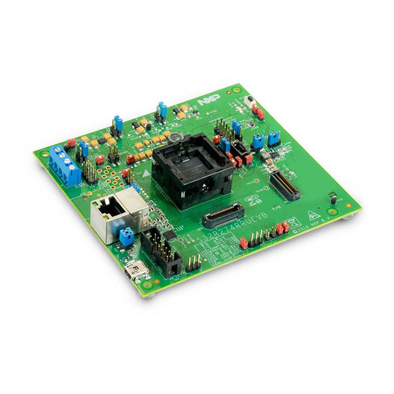
Page 14: Configuration - Daughter Card
The daughter card has been designed with ease of use in mind and has been segmented into functional blocks as shown in Figure 12. Detailed silkscreen legend has been used throughout the board to identify all switches, jumpers and user connectors. S32R274/372 EVB User Guide, Rev. 0, 08/2018 NXP Semiconductors... -
Page 15: Mcu Power
4.1.1. Supply routing and jumpers The different MCU supply inputs are connected to the regulators on the motherboard through the interface connector. Figure 13 shows how the MCU power domains are connected to the regulators. S32R274/372 EVB User Guide, Rev. 0, 08/2018 NXP Semiconductors... - Page 16 Table 8. MCU power selection jumpers Jumper Description Connects Digital HV supplies to 3.3V_SR Connects Digital LV supplies to 1.25V_SR Connects AFE Supply to 3.3V_LR via LDO Connects AFE Supply to 3.3V_SR via LDO S32R274/372 EVB User Guide, Rev. 0, 08/2018 NXP Semiconductors...
-
Page 17: Reset Circuit
RST-SW. Since the S32R274 device offers both internal and external regulation modes this is configurable on the daughtercard, and thus an external voltage monitoring IC (U18 – Linear Devices LTC2905) is utilised to protect the device when in external regulation mode and the device low voltage detect (LVD) mechanism is disabled. -
Page 18: Mcu External Clock Circuit
Eagle MR3003 RF front end board. The clock circuitry for the daughter card is shown in Figure 16. Each source is selectable via the 0-ohm links as shown, with crystal Y3 being the default factory option. S32R274/372 EVB User Guide, Rev. 0, 08/2018 NXP Semiconductors... -
Page 19: Jtag
Figure 16. 40MHz crystal circuit 4.4. JTAG The EVB is fitted with 14-pin JTAG debug connector. The following diagram shows the 14-pin JTAG connector pinout (0.1” keyed header). Figure 17. JTAG connector pinout S32R274/372 EVB User Guide, Rev. 0, 08/2018 NXP Semiconductors... -
Page 20: Nexus Aurora
Configuration – Daughter card 4.5. Nexus Aurora Table 10 shows the pinout of the 34-pin Samtec connector for the S32R274. Table 10. Aurora Trace connector pinout Pin No Function Pin No Function TX0+ VREF TX0- TCK/TCKC/DRC TMS/TMSC/TxD ataP TX1+ TDI/TxDataN... -
Page 21: Camera Serial Interface (Mipi-Csi2)
Figure 19. MIPI-CSI2 connector pinout 4.8. Gigabit Ethernet The S32R274RRUEVB daughtercard includes support for Gb ethernet, utilizing the RGMII interface present on the S32R274 device. The daughtercard is designed with a Micrel KSZ9031RNXUA Ethernet S32R274/372 EVB User Guide, Rev. 0, 08/2018 NXP Semiconductors... - Page 22 (U17), and associated RJ45 connector (J14 - Bel Fuse V890-1AX1-A1). This is the default configuration of the RGMII signals from the S32R274 device. If for any reason the alternate functions multiplexed on the RGMII pads are required then these signals can be routed to the motherboard by adding a 0-ohm link to the pads provided.
-
Page 23: Can Fd
Similarly CAN2 signals can be routed to either the on-board CAN-FD phy U16 via J43 and J44, or to the motherboard Flexray physical interface via J46 and J45. Figure 21. CAN FD physical interfaces S32R274/372 EVB User Guide, Rev. 0, 08/2018 NXP Semiconductors... -
Page 24: Test Points - Daughter Card
Surface Pad 320Mhz PLL 1.4V analog supply for VDD_LV_SDADC TP33 Surface Pad SD ADCs 1.4V analog supply for VDD_LV_OSC TP34 Surface Pad crystal oscillator 125MHz ENET ENET_REF_CLK TP35 Test Loop Reference clock S32R274/372 EVB User Guide, Rev. 0, 08/2018 NXP Semiconductors... -
Page 25: Configuring The Daughter Card For Standalone Use25
1.25 V PLL supply 3.3 V Flash supply 3.3 V ADC supply 3.3 V supply to MCU CAN2 Tx connection to PHY CAN2 Rx connection to PHY Flexray TXD A connection to motherboard S32R274/372 EVB User Guide, Rev. 0, 08/2018 NXP Semiconductors... -
Page 26: Configuring Internal Vreg Mode
3.3 V ADC supply 3.3 V supply to MCU CAN2 Tx connection to PHY CAN2 Rx connection to PHY Flexray TXD A connection to motherboard Flexray TXEN A connection to motherboard S32R274/372 EVB User Guide, Rev. 0, 08/2018 NXP Semiconductors... -
Page 27: Board Interface Connector
(such as the CAN and FlexRay). • Ground signals are not listed here. A solid ground connection is achieved through the middle bar of the interface connector. S32R274/372 EVB User Guide, Rev. 0, 08/2018 NXP Semiconductors... - Page 28 5.0V_SR 5.0V_SR 5.0V_SR GPIO 48 A-25 B-216 ADC1_AN_3 (FLEX_TXD_A_PD0) A-26 B-215 ADC0_AN_2 A-27 B-214 ADC0_AN_3 A-28 B-213 A-29 B-212 A-30 B-211 GPIO 53 (PD5) A-31 B-210 GPIO 54 (PD6) A-32 B-209 S32R274/372 EVB User Guide, Rev. 0, 08/2018 NXP Semiconductors...
- Page 29 (GPIO_PE15) A-61 1.25V_SR B-180 1.25V_SR 1.25V_SR 1.25V_SR A-62 1.25V_SR B-179 1.25V_SR 1.25V_SR 1.25V_SR A-63 1.25V_SR B-178 1.25V_SR 1.25V_SR 1.25V_SR A-64 1.25V_SR B-177 1.25V_SR 1.25V_SR 1.25V_SR A-65 B-176 FCCU_F_0 GPIO 116 (PH4) S32R274/372 EVB User Guide, Rev. 0, 08/2018 NXP Semiconductors...
- Page 30 A-87 B-154 GPIO 130 (GPIO_PI2) (I2C1_DATA) A-88 B-153 GPIO 121 (GPIO_PH9) A-89 B-152 A-90 B-151 A-91 B-150 A-92 B-149 A-93 B-148 A-94 B-147 A-95 PI10 B-146 PJ10 A-96 PI11 B-145 PJ11 S32R274/372 EVB User Guide, Rev. 0, 08/2018 NXP Semiconductors...
- Page 31 5.0V_LR B-119 5.0V_LR 5.0V_LR 5.0V_LR A-123 5.0V_LR B-118 5.0V_LR 5.0V_LR 5.0V_LR A-124 5.0V_LR B-117 5.0V_LR 5.0V_LR 5.0V_LR A-125 B-116 A-126 B-115 A-127 B-114 A-128 B-113 A-129 B-112 A-130 B-111 A-131 B-110 S32R274/372 EVB User Guide, Rev. 0, 08/2018 NXP Semiconductors...
- Page 32 PO15 B-81 PP15 A-161 1.25V_SR B-80 1.25V_SR 1.25V_SR 1.25V_SR A-162 1.25V_SR B-79 1.25V_SR 1.25V_SR 1.25V_SR A-163 1.25V_SR B-78 1.25V_SR 1.25V_SR 1.25V_SR A-164 1.25V_SR B-77 1.25V_SR 1.25V_SR 1.25V_SR A-165 B-76 A-166 B-75 S32R274/372 EVB User Guide, Rev. 0, 08/2018 NXP Semiconductors...
- Page 33 B-47 A-195 PS10 B-46 PT10 A-196 PS11 B-45 PT11 A-197 PS12 B-44 PT12 A-198 PS13 B-43 PT13 A-199 PS14 B-42 PT14 A-200 PS15 B-41 PT15 A-201 3.3V_SR B-40 3.3V_SR 3.3V_SR 3.3V_SR S32R274/372 EVB User Guide, Rev. 0, 08/2018 NXP Semiconductors...
- Page 34 VDD_HV_IO_MAIN VDD_HV_IO_MAIN A-224 B-17 3.3v_SR_LDO 3.3v_SR_LDO VDD_HV_IO_MAIN VDD_HV_IO_MAIN A-225 B-16 A-226 B-15 A-227 B-14 A-228 B-13 A-229 B-12 A-230 B-11 A-231 B-10 A-232 A-233 A-234 A-235 PW10 PX10 A-236 PW11 PX11 S32R274/372 EVB User Guide, Rev. 0, 08/2018 NXP Semiconductors...
-
Page 35: Default Jumper Summary Table
Table 15. Default jumper table - motherboard Jumper Default Pos PCB Legend Description MASTER LIN Master/Slave select CAP A DIS Disable capacitor circuitry for FlexRAY_A signals CAP A DIS Disable capacitor circuitry for S32R274/372 EVB User Guide, Rev. 0, 08/2018 NXP Semiconductors... - Page 36 7-8: GND to WAKE FlexRAY transceiver VIO selection FR_PWR 1-2: 12V to V 3-4: 5V_SR to V and V 1-2: PHY U5 TX to MCU FR_B 3-4: PHY U5 TXEN to MCU S32R274/372 EVB User Guide, Rev. 0, 08/2018 NXP Semiconductors...
- Page 37 Ethernet signal: COL_PHYAD0 Ethernet signal: TXEN Ethernet signal: TXCLK Ethernet signal: TXD0 Ethernet signal: TXD1 Ethernet signal: TXD2 Ethernet signal: TXD3_SNIMODE Ethernet signal: MDC Ethernet signal: MDIO Connect RV1 to analug input AN0 S32R274/372 EVB User Guide, Rev. 0, 08/2018 NXP Semiconductors...
-
Page 38: User Area
The P12V rail from the 12 V input is scaled to 4.3 V through the voltage divider of R81 and R82 and the scaled voltage can be connected to PB[5] via J55. 6.3. Known issues No known issues. S32R274/372 EVB User Guide, Rev. 0, 08/2018 NXP Semiconductors... - Page 40 EU and/or elsewhere. All rights reserved. Oracle and Java are registered trademarks of Oracle and/or its affiliates. The Power Architecture and Power.org word marks and the Power and Power.org logos and related marks are trademarks and service marks licensed by Power.org. © 2017 NXP B.V. Document Number: S32R274/372EVBUG Rev. 0 08/2018...
Need help?
Do you have a question about the S32R274 and is the answer not in the manual?
Questions and answers