Table of Contents
Advertisement
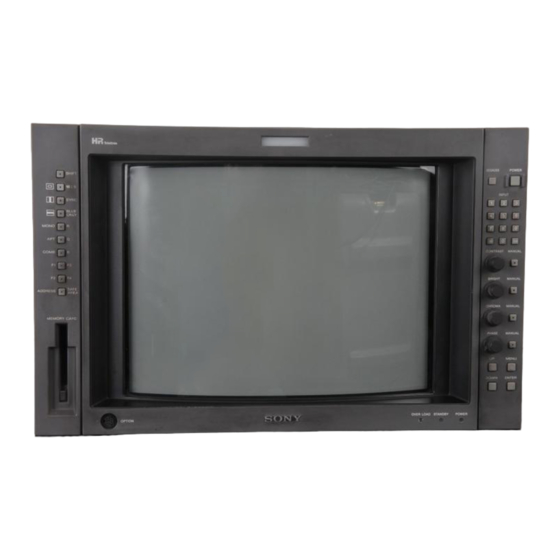
TRINITRON
COLOR VIDEO MONITOR
®
BVM-14G1A/14G1E/14G1U
BVM-14G5A/14G5E/14G5U
BVM-20G1A/20G1E/20G1U
MONITOR CONTROL UNIT
BKM-10R
OPERATION AND MAINTENANCE MANUAL [English]
1st Edition
Serial No. 2000001 and Higher
CHASSIS No. SCC-N52D-A (AUS)/J32H-A (AEP)/H99J-A (U/C)
CHASSIS No. SCC-N52E-A (AUS)/J32J-A (AEP)/H99K-A (U/C)
CHASSIS No. SCC-N52C-A (AUS)/J32G-A (AEP)/H99H-A (U/C)
Advertisement
Table of Contents


Need help?
Do you have a question about the TRINITRON BVM-14G1A and is the answer not in the manual?
Questions and answers