
Related Manuals for Atmel AT91SAM9263-EK


Summary of Contents for Atmel AT91SAM9263-EK
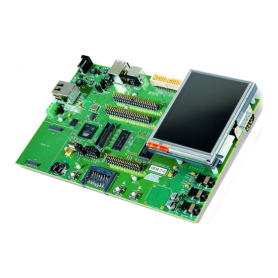
- Page 1 AT91SAM9263-EK Evaluation Board Rev. B ........................User Guide 6341B–ATARM–17-Sep-08...
-
Page 3: Table Of Contents
How to Identify the SAM9263 Silicon Revision ..............1-2 NAND Flash Access Issue....................1-3 Deliverables ........................1-3 AT91SAM9263-EK Evaluation Board Rev. B ..............1-4 Section 2 Setting Up the AT91SAM9263-EK Board Rev. B............2-1 Electrostatic Warning ......................2-1 Requirements........................2-1 Layout ..........................2-1 Powering Up the Board...................... 2-4 Backup Power Supply...................... - Page 4 Configuration Jumpers and Straps ..................4-1 Section 5 Schematics......................... 5-1 Schematics ........................5-1 Section 6 Warning ........................6-1 BMS Signal Sampling ......................6-1 Section 7 Revision History ......................7-1 Revision History ......................... 7-1 AT91SAM9263-EK Evaluation Board Rev. B User Guide 6341B–ATARM–17-Sep-08...
-
Page 5: Overview
Section 1 Overview Scope The AT91SAM9263-EK evaluation kit enables the evaluation of and code development for applications running on an AT91SAM9263. This guide focuses on the AT91SAM9263-EK board Rev. B as an evaluation platform. How to Identify the Kit BOM Revision Table 1-1. -
Page 6: How To Identify The Pcb Revision
How to Identify the SAM9263 Silicon Revision The AT91SAM9263 MRL B (Marketing Revision Level B) parts are identified with a letter “B” on top of the package as shown below: Figure 1-2. AT91SAM92639263 MRL B AT91SAM9263-EK Evaluation Board Rev. B User Guide 6341B–ATARM–17-Sep-08... -
Page 7: Nand Flash Access Issue
Overview NAND Flash Access Issue On the AT91SAM9263-EK with Kit BOM revision 007, the user can experience access errors when read- ing or writing the NAND Flash device (MN21B). This problem is due to disturbances on the chip select line. It can be fixed by the following:... -
Page 8: At91Sam9263-Ek Evaluation Board Rev. B
Two user input push buttons One Wakeup input push button One reset push button ® One DataFlash /SD/SDIO/MMC card slot One SD/SDIO/MMC card slot One Lithium Coin Cell Battery Retainer for 12 mm cell size AT91SAM9263-EK Evaluation Board Rev. B User Guide 6341B–ATARM–17-Sep-08... -
Page 9: Setting Up The At91Sam9263-Ek Board Rev. B
Avoid touching the component pins or any other metal- lic element. Requirements In order to set up the AT91SAM9263-EK evaluation board Rev. B, the following items are needed: the AT91SAM9263-EK evaluation board Rev. B itself AC/DC power adapter (12V at 1A), 2.1 mm by 5.5 mm... - Page 10 Setting Up the AT91SAM9263-EK Board Rev. B Figure 2-1. AT91SAM9263-EK Layout - Top View AT91SAM9263-EK Evaluation Board Rev. B User Guide 6341B–ATARM–17-Sep-08...
- Page 11 Setting Up the AT91SAM9263-EK Board Rev. B Figure 2-2. AT91SAM9263-EK Layout - Bottom View AT91SAM9263-EK Evaluation Board Rev. B User Guide 6341B–ATARM–17-Sep-08...
-
Page 12: Powering Up The Board
Setting Up the AT91SAM9263-EK Board Rev. B Powering Up the Board The AT91SAM9263-EK requires 12V DC. DC power is supplied to the board via the 2.1 mm by 5.5 mm socket J1. Coaxial plug center positive standard. Backup Power Supply The user has the possibility to plug a battery (3V Lithium Battery CR1225 or equivalent) in order to per- manently power the backup part of the device. -
Page 13: At91Sam9263-Ek Block Diagram
Setting Up the AT91SAM9263-EK Board Rev. B AT91SAM9263-EK Block Diagram Figure 2-3. AT91SAM9263-EK Block Diagram AT91SAM9263-EK Evaluation Board Rev. B User Guide 6341B–ATARM–17-Sep-08... -
Page 14: Board Description
Image Sensor Interface – ITU-R BT. 601/656 External Interface, Programmable Frame Capture Rate – 12-bit Data Interface for Support of High Sensibility Sensors – SAV and EAV Synchronization, Preview Path with Scaler, YCbCr Format AT91SAM9263-EK Evaluation Board Rev. B User Guide 6341B–ATARM–17-Sep-08... - Page 15 – 160 Programmable I/O Lines Multiplexed with Up to Two Peripheral I/Os – Input Change Interrupt Capability on Each I/O Line – Individually Programmable Open-drain, Pull-up Resistor and Synchronous Output One Part 2.0A and Part 2.0B-compliant CAN Controller AT91SAM9263-EK Evaluation Board Rev. B User Guide 6341B–ATARM–17-Sep-08...
- Page 16 – 3.0V to 3.6V for VDDOSC, VDDPLL and VDDIOP0 (Peripheral I/Os) – 1.65V to 3.6V for VDDIOP1 (Peripheral I/Os) – Programmable 1.65V to 1.95V or 3.0V to 3.6V for VDDIOM0/VDDIOM1 (Memory I/Os) Available in a 324-ball BGA Green Package AT91SAM9263-EK Evaluation Board Rev. B User Guide 6341B–ATARM–17-Sep-08...
-
Page 17: At91Sam9263 Block Diagram
Board Description AT91SAM9263 Block Diagram Figure 3-1. AT91SAM9263 Block Diagram AT91SAM9263-EK Evaluation Board Rev. B User Guide 6341B–ATARM–17-Sep-08... -
Page 18: Memory
128 Kbytes of Internal ROM 80 Kbytes of Internal single-cycle access high-speed SRAM 16 Kbytes of Internal single-cycle access high-speed SRAM 8 Mbytes of Atmel NOR Flash (not populated) 64 Mbytes of SDRAM memory 4 Mbytes of PSRAM (EBI1) 256 Mbytes of NAND Flash memory... -
Page 19: Audio Stereo Interface
One DataFlash/SD/SDIO/MMC card slot One SD/SDIO/MMC card slot All unused I/Os of the AT91SAM9263 are routed to peripheral extension connectors (J24 and J25). This allows the developer to add external hardware components or boards. AT91SAM9263-EK Evaluation Board Rev. B User Guide 6341B–ATARM–17-Sep-08... -
Page 20: Pio Usage
PA29 CTS0 EBI1_D29 RS232 COM PORT (J15) CTS0 VDDIOM1 PA30 SCK0 EBI1_D30 LCD PANEL (Power Control In) PA30 as PCI VDDIOM1 PA31 DMARQ0 EBI_D31 TOUCH SCREEN CONTROLLER (MN19) PA31 as BUSY VDDIOM1 AT91SAM9263-EK Evaluation Board Rev. B User Guide 6341B–ATARM–17-Sep-08... - Page 21 TIOB2 VDDIOP0 PB19 VDDIOP0 PB20 VDDIOP0 PB21 VDDIOP0 PB22 VDDIOP0 PB23 VDDIOP0 PB24 DMARQ3 VDDIOP0 PB25 VDDIOP0 PB26 VDDIOP0 PB27 PWM2 VDDIOP0 PB28 TCLK0 VDDIOP0 PB29 PWM3 VDDIOP0 PB30 VDDIOP0 PB31 VDDIOP0 AT91SAM9263-EK Evaluation Board Rev. B User Guide 6341B–ATARM–17-Sep-08...
- Page 22 VDDIOP0 PC28 PWM0 TCLK1 VDDIOP0 PC29 PCK0 PWM2 USER'S LED2 CONTROL (DS2) PC29 or PWM2 VDDIOP0 PC30 DRXD SERIAL DEBUG PORT (J14) DRXD VDDIOP0 PC31 DTXD SERIAL DEBUG PORT (J14) DTXD VDDIOP0 AT91SAM9263-EK Evaluation Board Rev. B User Guide 6341B–ATARM–17-Sep-08...
- Page 23 EBI0_D28 TPK12 EBI0 SDRAM DATA BUS VDDIOM0 PD29 EBI0_D29 TPK13 EBI0 SDRAM DATA BUS VDDIOM0 PD30 EBI0_D30 TPK14 EBI0 SDRAM DATA BUS VDDIOM0 PD31 EBI0_D31 TPK15 EBI0 SDRAM DATA BUS VDDIOM0 3-10 AT91SAM9263-EK Evaluation Board Rev. B User Guide 6341B–ATARM–17-Sep-08...
- Page 24 ETHERNET RMII (MN18) ETXEN VDDIOM1 PE29 EMDC EBI1_CAS ETHERNET RMII (MN18) EMDC VDDIOM1 PE30 EMDIO EBI1_SDWE ETHERNET RMII (MN18) EMDIO VDDIOM1 PE31 EF100 EBI1_SDA10 ETHERNET RMII (MN18) PE31 as IRQ VDDIOM1 AT91SAM9263-EK Evaluation Board Rev. B User Guide 3-11 6341B–ATARM–17-Sep-08...
-
Page 25: Configuration
Enables the use of the SERIAL EEPROM SDA (PB4) Enables the use of the DBGU TXD signal (PC31) Enables the use of the DBGU RXD signal (PC30) Enables the use of the USB CNX detection (PA25) AT91SAM9263-EK Evaluation Board Rev. B User Guide 6341B–ATARM–17-Sep-08... - Page 26 AGND of TP72 Note: 1. These jumpers are provided for power consumption measurement use. By default, they are closed. To use this feature, the user has to open the strap and insert an ammeter. AT91SAM9263-EK Evaluation Board Rev. B User Guide 6341B–ATARM–17-Sep-08...
-
Page 27: Schematics
Section 5 Schematics Schematics This section contains the following schematics: AT91SAM9263-EK Diagram Power Supply AT91SAM9263 EBI0 Memory EBI1 Memory Serial Memory Audio AC97 Serial Interfaces Ethernet LCD and ISI Expansion AT91SAM9263-EK Evaluation Board Rev. B User Guide 6341B–ATARM–17-Sep-08... -
Page 28: Ebi0 Memory
DES. DES. DES. DATE DATE DATE VER. VER. VER. DATE DATE DATE PA30 (PCI) PB30 PC30 DRXD PD30 PE30 EMDIO AT91SAM9263-EK AT91SAM9263-EK AT91SAM9263-EK SCALE SCALE SCALE REV. REV. REV. SHEET SHEET SHEET PA31 (BUSY) PB31 PC31 DTXD PD31 PE31 (MDINTR) - Page 29 MODIF. MODIF. MODIF. DES. DES. DES. DATE DATE DATE VER. VER. VER. DATE DATE DATE AT91SAM9263-EK AT91SAM9263-EK AT91SAM9263-EK SCALE SCALE SCALE REV. REV. REV. SHEET SHEET SHEET POWER SUPPLY POWER SUPPLY POWER SUPPLY This agreement is our property. Reproduction and publication without our written authorization shall expose offender to legal proceedings.
- Page 30 10-OCT-06 10-OCT-06 SHDN MODIF. MODIF. MODIF. DES. DES. DES. DATE DATE DATE VER. VER. VER. DATE DATE DATE AT91SAM9263-EK AT91SAM9263-EK AT91SAM9263-EK SCALE SCALE SCALE REV. REV. REV. SHEET SHEET SHEET NRST AT91SAM9263 AT91SAM9263 AT91SAM9263 NRST WAKE UP This agreement is our property. Reproduction and publication without our written authorization shall expose offender to legal proceedings.
- Page 31 MODIF. MODIF. MODIF. DES. DES. DES. DATE DATE DATE VER. VER. VER. DATE DATE DATE AT91SAM9263-EK AT91SAM9263-EK AT91SAM9263-EK SCALE SCALE SCALE REV. REV. REV. SHEET SHEET SHEET EBI0 MEMORY EBI0 MEMORY EBI0 MEMORY This agreement is our property. Reproduction and publication without our written authorization shall expose offender to legal proceedings.
- Page 32 MODIF. MODIF. MODIF. DES. DES. DES. DATE DATE DATE VER. VER. VER. DATE DATE DATE AT91SAM9263-EK AT91SAM9263-EK AT91SAM9263-EK SCALE SCALE SCALE REV. REV. REV. SHEET SHEET SHEET EBI1 MEMORY EBI1 MEMORY EBI1 MEMORY This agreement is our property. Reproduction and publication without our written authorization shall expose offender to legal proceedings.
- Page 33 MODIF. MODIF. MODIF. DES. DES. DES. DATE DATE DATE VER. VER. VER. DATE DATE DATE AT91SAM9263-EK AT91SAM9263-EK AT91SAM9263-EK SCALE SCALE SCALE REV. REV. REV. SHEET SHEET SHEET MCI & TWI MCI & TWI MCI & TWI This agreement is our property. Reproduction and publication without our written authorization shall expose offender to legal proceedings.
- Page 34 MODIF. DES. DES. DES. DATE DATE DATE VER. VER. VER. DATE DATE DATE USING VREFH BIT (REG 76h) AGND_AC97 AT91SAM9263-EK AT91SAM9263-EK AT91SAM9263-EK SCALE SCALE SCALE REV. REV. REV. SHEET SHEET SHEET AUDIO AC97 AUDIO AC97 AUDIO AC97 This agreement is our property. Reproduction and publication without our written authorization shall expose offender to legal proceedings.
-
Page 35: Serial Interfaces
MODIF. MODIF. MODIF. DES. DES. DES. DATE DATE DATE VER. VER. VER. DATE DATE DATE AT91SAM9263-EK AT91SAM9263-EK AT91SAM9263-EK SCALE SCALE SCALE REV. REV. REV. SHEET SHEET SHEET SERIAL INTERFACES SERIAL INTERFACES SERIAL INTERFACES This agreement is our property. Reproduction and publication without our written authorization shall expose offender to legal proceedings. - Page 36 MODIF. MODIF. MODIF. DES. DES. DES. DATE DATE DATE VER. VER. VER. DATE DATE DATE AT91SAM9263-EK AT91SAM9263-EK AT91SAM9263-EK SCALE SCALE SCALE REV. REV. REV. SHEET SHEET SHEET RMII ETHERNET RMII ETHERNET RMII ETHERNET This agreement is our property. Reproduction and publication without our written authorization shall expose offender to legal proceedings.
- Page 37 MODIF. MODIF. MODIF. DES. DES. DES. DATE DATE DATE VER. VER. VER. DATE DATE DATE AT91SAM9263-EK AT91SAM9263-EK AT91SAM9263-EK SCALE SCALE SCALE REV. REV. REV. SHEET SHEET SHEET LCD & ISI LCD & ISI LCD & ISI This agreement is our property. Reproduction and publication without our written authorization shall expose offender to legal proceedings.
- Page 38 MODIF. MODIF. MODIF. DES. DES. DES. DATE DATE DATE VER. VER. VER. DATE DATE DATE AT91SAM9263-EK AT91SAM9263-EK AT91SAM9263-EK SCALE SCALE SCALE REV. REV. REV. SHEET SHEET SHEET EXPANSION CONNECTORS EXPANSION CONNECTORS EXPANSION CONNECTORS This agreement is our property. Reproduction and publication without our written authorization shall expose offender to legal proceedings.
-
Page 39: Warning
AT91SAM9263 microcontroller samples the BMS signal one Slow Clock (SLCK) cycle after the NRST signal rising (See Figure 6-1). As a result, the BMS signal is sampled at a Low Level and the AT91SAM9263 boots out of the external EBI device connected to NCS0. AT91SAM9263-EK Evaluation Board Rev. B User Guide 6341B–ATARM–17-Sep-08... - Page 40 ROM: 1. Close J2 to force power on 2. Open J5 (Boot Mode Select Jumper) 3. Power on the board 4. Remove and replace J4-1 (VDDBU/VDDBACKUP Jumper) AT91SAM9263-EK Evaluation Board Rev. B User Guide 6341B–ATARM–17-Sep-08...
-
Page 41: Revision History
Section 5.1, ” Schematics” , updated with rev C schematics. 5626 (“Audio AC97” schematic updated) 5082 Table 4-1, “Configuration Jumpers and Straps,” on page 4-1 , added J5-7 and J29 5391. 6341A First issue. AT91SAM9263-EK Evaluation Board Rev. B User Guide 6341B–ATARM–17-Sep-08... - Page 42 Disclaimer: The information in this document is provided in connection with Atmel products. No license, express or implied, by estoppel or otherwise, to any intellectual property right is granted by this document or in connection with the sale of Atmel products. EXCEPT AS SET FORTH IN ATMEL’S TERMS AND CONDI- TIONS OF SALE LOCATED ON ATMEL’S WEB SITE, ATMEL ASSUMES NO LIABILITY WHATSOEVER AND DISCLAIMS ANY EXPRESS, IMPLIED OR STATUTORY...
Need help?
Do you have a question about the AT91SAM9263-EK and is the answer not in the manual?
Questions and answers