
Related Manuals for Atmel AT91SAM9M10-G45-EK


Summary of Contents for Atmel AT91SAM9M10-G45-EK
- Page 1 AT91SAM9M10-G45-EK ........................User Guide 6495B–ATARM–21-Apr-10...
-
Page 2: Table Of Contents
Software Controlled LEDs ................. 4-18 4.2.10 Serial Peripheral Interface Controller (SPI) ............4-19 4.2.11 Two Wire Interface (TWI)................... 4-19 4.2.12 SD/MMC Interface ..................... 4-19 4.2.13 TFT LCD with Touch Panel ................4-20 4.2.14 Push Buttons ..................... 4-22 AT91SAM9M10-G45-EK User Guide 6495B–ATARM–21-Apr-10... - Page 3 6.11 Image Sensor - ISI ......................6-9 6.12 Video ..........................6-10 6.13 Display Devices........................ 6-10 6.13.1 TFT LCD ......................6-10 6.14 LCD Extension ......................... 6-11 Section 7 Schematics .........................7-1 Schematics......................... 7-1 Section 8 Revision History......................8-1 Revision History ......................... 8-1 1-ii AT91SAM9M10-G45-EK User Guide 6495B–ATARM–21-Apr-10...
-
Page 4: Introduction
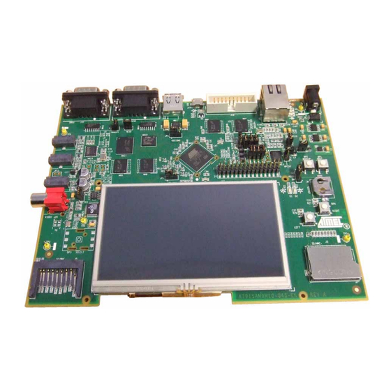
® The Atmel SAM9M10-G45-EK is a fully-featured evaluation platform for the Atmel AT91SAM9M10 or AT91SAM9G45 microcontroller. The kit is equipped with an AT91SAM9M10 chip, which is a superset of the AT91SAM9G45, and therefore allows evaluating that reference as well. The evaluation kit allows users to extensively evaluate, prototype and create application-specific designs. -
Page 5: Applicable Documents
Title Comments This document describes the SAM9G45, which is part of the ® Atmel's Smart ARM Microcontrollers. Atmel Literature n° 6438 SAM9G45 Preliminary It is available from http://www.atmel.com/dyn/resources/prod_documents/doc6438.pdf This document describes the SAM9M10, which is part of the ® Atmel Literature n° 6355... -
Page 6: Kit Contents
– One serial RS232 cable – One RJ45 crossed cable A Welcome Letter Figure 2-1. Unpacked SAM9M10-G45-EK Unpack and inspect this kit carefully. Contact your local Atmel distributor, should you have issues con- cerning the contents of the kit. AT91SAM9M10-G45-EK User Guide 6495B–ATARM–21-Apr-10... -
Page 7: Evaluation Board Specifications
We strongly recommend using a grounding strap or sim- ilar ESD protective device when handling the board in hostile ESD environments (offices with synthetic carpet, for example...). Avoid touching the component pins or any other metallic element on the board. AT91SAM9M10-G45-EK User Guide 6495B–ATARM–21-Apr-10... -
Page 8: Power Up
SAM9M10-G45-EK. Optionally, if you have a SAM-ICE™, instructions are also given about how to debug the code. We recommend that you backup the “SAM9M10-G45-EK DevStart” folder on your computer before launching it. AT91SAM9M10-G45-EK User Guide 6495B–ATARM–21-Apr-10... -
Page 9: Recovery Procedure
The DevStart ends by giving step-by-step instructions on how to recover the SAM9M10-G45-EK to the state as it was when shipped by Atmel. Follow the instructions if you deleted the contents of the NAND Flash and want to recover from this situation. -
Page 10: Board Description
DDR2/LPDDR memory interface is connected to 128 MB DDR2-SDRAM memory External Bus Interface (EBI) is connected to three kinds of memory devices (DDR2-SDRAM, NAND Flash and NOR Flash (not populated)) AT91SAM9M10-G45-EK User Guide 6495B–ATARM–21-Apr-10... -
Page 11: Board Interface Connection
Main power supply (J2) 4.1.3 Push Button Switches Reset, board reset (BP1) Wake up, push button to bring processor out of low power mode (BP2) Right and left click, user push button switches (BP4 and BP5) Joystick (BP3) AT91SAM9M10-G45-EK User Guide 6495B–ATARM–21-Apr-10... -
Page 12: Display Lcd And Leds
4.2.1 Processor The board features the Atmel SAM9M10-CU 324-ball TFBGA package. This chip runs at a nominal fre- quency of 400 MHz for the core and 133 MHz for the system bus. For more information, refer to the latest SAM9M10 datasheet available from http://www.atmel.com/... -
Page 13: Clock Circuitry
The chip selects NCS0, NCS1 and NCS3 are used for NOR Flash, DDR2-SDRAM and NAND Flash memories, respectively. Furthermore, a dedicated jumper can disconnect each of the two NCS0 and NCS3 signals, making them available for other functions. AT91SAM9M10-G45-EK User Guide 6495B–ATARM–21-Apr-10... - Page 14 Board Description Figure 4-3. EBI0 - DDR2 AT91SAM9M10-G45-EK User Guide 6495B–ATARM–21-Apr-10...
- Page 15 Board Description Figure 4-4. EBI1 - DDR2 + Flash AT91SAM9M10-G45-EK User Guide 6495B–ATARM–21-Apr-10...
-
Page 16: Power Supplies
LDO RT9186A series. It is powered by the output of the 3.3 VDC Supply. Note: 1. Corresponding test points (TP1 to TP4, GND) are used with jumpers (JP1.1 to JP7) to permit probing of these voltages. AT91SAM9M10-G45-EK User Guide 6495B–ATARM–21-Apr-10... - Page 17 2.2u 2.2u J1-4 J1-4 100k 100k 10uH 10uH VDDPLLUTMI RT9186A RT9186A 1V_VDDUTMIC VOUT VOUT 100n 100n PGOOD 4.7u 4.7u 100k 100k 10uH 10uH VDDPLLA 100n 100n 4.7u 4.7u J1-3 J1-3 VDDCORE VDDIOM0 VDDIOM1 100n 100n VDDBU AT91SAM9M10-G45-EK User Guide 6495B–ATARM–21-Apr-10...
- Page 18 RT9018A PGOOD VOUT DC POWER JACK DC POWER JACK PWR_EN 100k 100k Si1563EDH Si1563EDH 100k 100k SIP2 SIP2 RT9018A RT9018A FORCE POWER PGOOD VOUT SHDN 100k 100k RT9186A RT9186A VOUT VOUT R199 R199 PGOOD 100k 100k AT91SAM9M10-G45-EK User Guide 6495B–ATARM–21-Apr-10...
-
Page 19: Debug Interface
DBGU Com Port MN15 MN15 C158 100n C158 100n C159 C159 SERIAL DEBUG PORT 100n 100n C157 100n C157 100n C163 C163 100n 100n 100k 100k 100k 100k C165 100n C165 100n PB13 PB12 ADM3202ARNZ ADM3202ARNZ 4-10 AT91SAM9M10-G45-EK User Guide 6495B–ATARM–21-Apr-10... - Page 20 USB Device High speed and connected to the second UTMI port. One USB high/full speed type standard A connector One USB interface Host/Device Micro AB connector Refer to the SAM9M10 datasheet for detailed programming information. AT91SAM9M10-G45-EK User Guide 4-11 6495B–ATARM–21-Apr-10...
- Page 21 10Base-TX. The MII and RMII interfaces are capable of both 10Mb/s and 100Mb/s data rates as described in the IEEE 802.3u standard. The signals used by MII and RMII interfaces are described in the table below. 4-12 AT91SAM9M10-G45-EK User Guide 6495B–ATARM–21-Apr-10...
- Page 22 EMDC: management data clock clock EMDIO: management data EMDIO: management data EMDIO MDIO MDIO input / output input / output RESET# XT1 RESET# XT1 NRST NRST: microcontroller reset NRST: microcontroller reset (25 MHz) (REF_CLK 50MHz) AT91SAM9M10-G45-EK User Guide 4-13 6495B–ATARM–21-Apr-10...
- Page 23 Board Description Figure 4-11. Ethernet Port For more information about the Ethernet controller device, refer to the Davicom DM9161 controller man- ufacturer's datasheet. 4-14 AT91SAM9M10-G45-EK User Guide 6495B–ATARM–21-Apr-10...
-
Page 24: Audio Stereo Interface
The SAM9M10-G45-EK includes a WM9711L AC97 CODEC for digital sound input and output. This interface includes audio jacks for MIC input (J9), line audio input (J8), headphone line output (J7) and a 2-point speaker output connector (JP15). It is compliant with AC97 Component Specification V2.2. AT91SAM9M10-G45-EK User Guide 4-15 6495B–ATARM–21-Apr-10... - Page 25 220ohm at 100MHz 220ohm at 100MHz C155 C155 C156 C156 470p 470p 470p 470p STEREO_3.5mm STEREO_3.5mm AGND_AC97 AGND_AC97 For more information about the AC97 codec device, refer to the Wolfson WM9711L controller manufac- turer's datasheet. 4-16 AT91SAM9M10-G45-EK User Guide 6495B–ATARM–21-Apr-10...
-
Page 26: Tv-Out Extension
R182 R182 100p 100p PA20 (TWCK0) R183 75R R183 75R PA21 BAT54SLT1G BAT54SLT1G C/CVBS NRST RESET P-OUT R184 R184 R185 R185 13MHz 13MHz R186 R186 C207 C207 100n 100n 13MHz 13MHz C208 C208 C209 C209 AT91SAM9M10-G45-EK User Guide 4-17 6495B–ATARM–21-Apr-10... -
Page 27: Software Controlled Leds
Figure 4-14. Software Controlled LEDs USER INTERFACE Green Green 470R 470R 470R 470R PD31 Green Green 470R 470R PB15 PB16 100k 100k PB14 LEFT RIGHT PB18 PUSH DOWN JOYSTICK IRLML2402 IRLML2402 PB17 PD30 100R 100R PB[14..18] POWER LED 4-18 AT91SAM9M10-G45-EK User Guide 6495B–ATARM–21-Apr-10... -
Page 28: Serial Peripheral Interface Controller (Spi)
SD/MMC card slot. The second interface is used as a 4-bit interface (MCI0), connected to a 4-bit SD/MMC card slot. The users must provide their own compatible cards for use with these connectors. Please note that the power is connected to VCC, which is 3.3 volts. AT91SAM9M10-G45-EK User Guide 4-19 6495B–ATARM–21-Apr-10... -
Page 29: Tft Lcd With Touch Panel
The back light voltage is generated from a CP2122ST boost converter. It is powered directly by the VIN 5 VCC power (the control for the back light voltages is separated from the main board voltages due to the specific voltage requirements of the LCD panel). 4-20 AT91SAM9M10-G45-EK User Guide 6495B–ATARM–21-Apr-10... - Page 30 9 LEDs Back Light R149 R149 PE12 RED7 R148 R148 PE14 R147 R147 PE11 RED6 R146 R146 PE13 R145 R145 PE10 RED5 R144 R144 PE12 R184 R184 RED4 R183 R183 PE11 R182 R182 RED3 R181 R181 PE10 AT91SAM9M10-G45-EK User Guide 4-21 6495B–ATARM–21-Apr-10...
-
Page 31: Push Buttons
All I/Os of the SAM9M10 Image Sensor Interface are routed to connectors J17 Touch screen signals and analog I/O are connected to J18 This allows the developer to extend the features of the board by adding external hardware components or boards. 4-22 AT91SAM9M10-G45-EK User Guide 6495B–ATARM–21-Apr-10... - Page 32 HDR_2x10_SMT IMAGE SENSOR CONNECTOR C211 C211 C212 C212 C210 C210 100n 100n 100n 100n VDDISI PD12 PD13 PA21 PA20 PB31 PB29 PB30 PB28 PB20 PB21 PB22 PB23 PB24 PB25 PB26 PB27 PB10 PB11 HDR_2x15_SMT HDR_2x15_SMT AT91SAM9M10-G45-EK User Guide 4-23 6495B–ATARM–21-Apr-10...
-
Page 33: Configuration
Disables TCK <-> RTCK local loop ETHERNET Configuration RMII is the factory default mode. To evaluate the MII mode, the user has to unsolder R99 and solder R100, R103 to R105, R108 to R110, R112, R114, C174, C175, Y5. AT91SAM9M10-G45-EK User Guide 6495B–ATARM–21-Apr-10... -
Page 34: Jumpers Configuration
Set address A0 low (MN12 Serial EEPROM), enable Boot access. JP14 JP14.1 = Line_Out JP14.3 = AGND JP15 Used to connect a Loudspeaker JP16 Closed DISMDIX (MN18) JP17-JP18 Test points Give access to the four GPIOs of WM9711L AT91SAM9M10-G45-EK User Guide 6495B–ATARM–21-Apr-10... -
Page 35: Miscellaneous Configuration Items
A or B. The multiplexing tables in the following paragraphs define how the I/O lines of peripherals A and B are multiplexed on the PIO Controllers. 5.5.2 Multiplexing on PIO Controller A (PIOA) "R.Select" = connection selectable via an on-board resistor (default not populated) AT91SAM9M10-G45-EK User Guide 6495B–ATARM–21-Apr-10... - Page 36 MMCI1 Data4 Ethernet MII VDDIOP0 PA28 MCI1_DA5 ERXCK R.Select MMCI1 Data5 Ethernet MII VDDIOP0 PA29 MCI1_DA6 ECRS R.Select MMCI1 Data6 Ethernet MII VDDIOP0 PA30 MCI1_DA7 ECOL R.Select MMCI1 Data7 Ethernet MII VDDIOP0 PA31 MCI1_CK PCK0 MMCI1_clock VDDIOP0 AT91SAM9M10-G45-EK User Guide 6495B–ATARM–21-Apr-10...
-
Page 37: Multiplexing On Pio Controller B (Piob)
PB27 ISI_D7 Image Sensor Data 7 VDDIOP2 PB28 ISI_PCK Image Sensor Data Clock VDDIOP2 PB29 ISI_VSYNC Image Sensor Vertical Synchro VDDIOP2 PB30 ISI_HSYNC Image Sensor Horizontal Synchro VDDIOP2 PB31 ISI_MCK PCK1 Image Sensor Reference Clock VDDIOP2 AT91SAM9M10-G45-EK User Guide 6495B–ATARM–21-Apr-10... -
Page 38: Multiplexing On Pio Controller C (Pioc)
VDDIOM1 PC15 NWAIT VDDIOM1 PC16 VDDIOM1 PC17 VDDIOM1 PC18 VDDIOM1 PC19 VDDIOM1 PC20 VDDIOM1 PC21 VDDIOM1 PC22 VDDIOM1 PC23 VDDIOM1 PC24 VDDIOM1 PC25 VDDIOM1 PC26 VDDIOM1 PC27 VDDIOM1 PC28 VDDIOM1 PC29 VDDIOM1 PC30 VDDIOM1 PC31 VDDIOM1 AT91SAM9M10-G45-EK User Guide 6495B–ATARM–21-Apr-10... -
Page 39: Multiplexing On Pio Controller D (Piod)
General purpose A/D6 VDDIOP0 PD27 PCK1 SPI0_NPCS3 GPAD7 General purpose A/D7 VDDIOP0 PD28 TSADTRG SPI1_NPCS1 USB Plug-ID IDUSB VDDIOP0 PD29 TCLK1 SCK1 MCI1_WP VDDIOP0 PD30 TIOB0 SCK2 Command Power Led VDDIOP0 PD31 TIOB1 PWM1 Command LED1 VDDIOP0 AT91SAM9M10-G45-EK User Guide 6495B–ATARM–21-Apr-10... -
Page 40: Multiplexing On Pio Controller E (Pioe)
PE24 LCDD17 LCDD23 LCD-Blue1 VDDIOP1 PE25 LCDD18 LCD-Blue2 VDDIOP1 PE26 LCDD19 LCD-Blue3 VDDIOP1 PE27 LCDD20 LCD-Blue4 VDDIOP1 PE28 LCDD21 LCD-Blue5 VDDIOP1 PE29 LCDD22 LCD-Blue6 VDDIOP1 PE30 LCDD23 LCD-Blue7 VDDIOP1 PE31 PWM2 PCK1 AC97 External Clock VDDIOP1 AT91SAM9M10-G45-EK User Guide 6495B–ATARM–21-Apr-10... -
Page 41: Connectors
Power Supply Connector J2 Table 6-1. Power Supply Connector J2 Signal Description Mnemonic Signal description Center +5 VCC RS232 Connector with RTS/CTS Handshake Support Connector J11 is the COM1 connector. Figure 6-2. RS232 COM1 Connector J11 AT91SAM9M10-G45-EK User Guide 6495B–ATARM–21-Apr-10... -
Page 42: Dbgu
Table 6-3. RS232 DBGU Connector J10 Signal Descriptions Mnemonic Signal description 1, 4, 6, 7, 8, 9 NO CONNECTION TXD TRANSMITTED DATA RS232 serial data output signal RXD RECEIVED DATA RS232 serial data input signal GROUND AT91SAM9M10-G45-EK User Guide 6495B–ATARM–21-Apr-10... -
Page 43: Ethernet
Connector J12 is the USB Host connector. Figure 6-5. USB Host type A connector J12 Table 6-5. USB Host Type A Connector J12 Signal Descriptions Mnemonic Signal description Vbus 5v power Data minus Data plus Ground Shield Shield AT91SAM9M10-G45-EK User Guide 6495B–ATARM–21-Apr-10... -
Page 44: Usb Host/Device
Connector J13 is the JTAG/ICE connector. A SAM-ICE connector is a 20-way Insulation Displacement Connector (IDC) keyed box header (2.54 mm male) that mates with IDC sockets mounted on a ribbon cable. Figure 6-7. JTAG/ICE Connector J13 AT91SAM9M10-G45-EK User Guide 6495B–ATARM–21-Apr-10... - Page 45 CPU. Common ground nSRST RESET Active-low reset signal. Target CPU reset signal Common ground This pin is not connected in SAM-ICE. Common ground This pin is not connected in SAM-ICE Common ground AT91SAM9M10-G45-EK User Guide 6495B–ATARM–21-Apr-10...
-
Page 46: Sd/Mmc- Mci0
Connectors SD/MMC- MCI0 Connector J6 is the SD/MMC connector. Figure 6-8. SD/MMC0 Connector J6 Table 6-8. SD/MMC0 Connector J6 Signal Descriptions Mnemonic Mnemonic RSV/DAT3 DAT0 DAT1 DAT2 Card Detect AT91SAM9M10-G45-EK User Guide 6495B–ATARM–21-Apr-10... -
Page 47: Sd/Mmc- Mci1
Connectors SD/MMC- MCI1 Connector J5 is the SD/MMC connector. Figure 6-9. SD/MMC1 Connector J5 Table 6-9. SD/MMC1 Connector J5 Signal Descriptions Mnemonic Mnemonic RSV/DAT3 DAT0 DAT1 DAT2 DAT3 DAT4 DAT5 DAT6 DAT7 AT91SAM9M10-G45-EK User Guide 6495B–ATARM–21-Apr-10... -
Page 48: Ac97
Connector JP15 is the Speaker Output connector Figure 6-10. Audio Connector J7, J8, J9 Table 6-10. J7, J8, J9 Signal Description Mnemonic Signal Signal Table 6-11. Speaker JP15 Signal Descriptions Mnemonic Speaker bridge output A Speaker bridge output B AT91SAM9M10-G45-EK User Guide 6495B–ATARM–21-Apr-10... -
Page 49: Image Sensor - Isi
Figure 6-11. ISI Connector J17 Table 6-12. ISI Connector J17 Signal Descriptions Mnemonic Mnemonic VCC 3v3 VCC 3v3 Ctrl1 Ctrl2 ISI_MCK ISI_VSYNC ISI_HSYNC ISI_PCK ISI_Data0 ISI_Data1 ISI_Data2 ISI_Data3 ISI_Data4 ISI_Data5 ISI_Data6 ISI_Data7 ISI_Data8 ISI_Data9 ISI_Data10 ISI_Data11 AT91SAM9M10-G45-EK User Guide 6495B–ATARM–21-Apr-10... -
Page 50: Video
Composite video signal output 6.13 Display Devices 6.13.1 TFT LCD Connector J24 is the TFT-LCD connector. Figure 6-13. TFT LCD Connector J24 Table 6-14. TFT LCD Connector J24 Signal Descriptions Mnemonic Mnemonic VLED- VLED+ VDD 3V3 6-10 AT91SAM9M10-G45-EK User Guide 6495B–ATARM–21-Apr-10... -
Page 51: Lcd Extension
PE23 BLUE Data Signal (LSB) PE26 BLUE Data Signal PE25 BLUE Data Signal PE28 BLUE Data Signal PE27 BLUE Data Signal PE30 BLUE Data Signal (MSB) PE29 BLUE Data Signal LCDHSYNC LCDVSYNC LCDDOTCK (0V) (0V) AT91SAM9M10-G45-EK User Guide 6-11 6495B–ATARM–21-Apr-10... - Page 52 Table 6-16. Connector J18 Signal Description for an LCD Extension Mnemonic Mnemonic AD1XM AD0XP AD3YM AD2YP (0V) (0V) PD25 PD25 PD24 PD24 PD27 PD27 PD26 PD26 PD19 PD19 PD18 PD18 (0V) (0V) (0V) (0V) (0V) +3V3 power source +3V3 power source 6-12 AT91SAM9M10-G45-EK User Guide 6495B–ATARM–21-Apr-10...
- Page 53 This section contains the following schematics: Top Level view, block architecture of the design Power Supply SAM Processor Bus impedance adaptor Main memory EBI memory MCI & TWI Audio AC97 Serial interfaces Ethernet Video interfaces and LCD extension AT91SAM9M10-G45-EK User Guide 6495B–ATARM–21-Apr-10...
- Page 54 DATE PA13 RXD1 PA29 MCI1_DA6/CRS PB13 DTXD PB29 ISI_VSYNC PC13 NOT USED PC29 NOT USED PD13 CTRL2 PD29 (MCI1_WP) PE13 PE29 AT91SAM9M10-G45-EK AT91SAM9M10-G45-EK AT91SAM9M10-G45-EK SCALE SCALE SCALE REV. REV. REV. SHEET SHEET SHEET PA14 TX_EN PA30 MCI1_DA7/COL PB14 BP3_LEFT PB30...
- Page 55 MODIF. MODIF. MODIF. DES. DES. DES. DATE DATE DATE VER. VER. VER. DATE DATE DATE AT91SAM9M10-G45-EK AT91SAM9M10-G45-EK AT91SAM9M10-G45-EK SCALE SCALE SCALE REV. REV. REV. SHEET SHEET SHEET POW ER SUPPLY POW ER SUPPLY POW ER SUPPLY This agreement is our property. Reproduction and publication without our written authorization shall expose offender to legal proceedings.
- Page 56 DATE DATE DATE VER. VER. VER. DATE DATE DATE SG-BGA-CA89405MF SG-BGA-CA89405MF Closed NCS0 SIP2 SIP2 AT91SAM9M10-G45-EK AT91SAM9M10-G45-EK AT91SAM9M10-G45-EK SCALE SCALE SCALE REV. REV. REV. SHEET SHEET SHEET AT91SAM9M10 chip AT91SAM9M10 chip AT91SAM9M10 chip This agreement is our property. Reproduction and publication without our written authorization shall expose offender to legal proceedings.
- Page 57 EBI0_DQS1 EBI1_DQS1 MODIF. MODIF. MODIF. DES. DES. DES. DATE DATE DATE VER. VER. VER. DATE DATE DATE AT91SAM9M10-G45-EK AT91SAM9M10-G45-EK AT91SAM9M10-G45-EK SCALE SCALE SCALE REV. REV. REV. SHEET SHEET SHEET SDA10 EBI1_SDA10 RES.ARRAYS-EBI0_EBI1 RES.ARRAYS-EBI0_EBI1 RES.ARRAYS-EBI0_EBI1 This agreement is our property. Reproduction and publication without our written authorization shall expose offender to legal proceedings.
- Page 58 MODIF. MODIF. MODIF. DES. DES. DES. DATE DATE DATE VER. VER. VER. DATE DATE DATE AT91SAM9M10-G45-EK AT91SAM9M10-G45-EK AT91SAM9M10-G45-EK SCALE SCALE SCALE REV. REV. REV. SHEET SHEET SHEET EBI0_DDR2 EBI0_DDR2 EBI0_DDR2 This agreement is our property. Reproduction and publication without our written authorization shall expose offender to legal proceedings.
- Page 59 MODIF. MODIF. MODIF. DES. DES. DES. DATE DATE DATE VER. VER. VER. DATE DATE DATE AT91SAM9M10-G45-EK AT91SAM9M10-G45-EK AT91SAM9M10-G45-EK SCALE SCALE SCALE REV. REV. REV. SHEET SHEET SHEET EBI1_MEMORY EBI1_MEMORY EBI1_MEMORY This agreement is our property. Reproduction and publication without our written authorization shall expose offender to legal proceedings.
- Page 60 MODIF. MODIF. MODIF. DES. DES. DES. DATE DATE DATE VER. VER. VER. DATE DATE DATE AT91SAM9M10-G45-EK AT91SAM9M10-G45-EK AT91SAM9M10-G45-EK SCALE SCALE SCALE REV. REV. REV. SHEET SHEET SHEET MCI & TW I MCI & TW I MCI & TW I This agreement is our property. Reproduction and publication without our written authorization shall expose offender to legal proceedings.
- Page 61 MODIF. MODIF. MODIF. DES. DES. DES. DATE DATE DATE VER. VER. VER. DATE DATE DATE AT91SAM9M10-G45-EK AT91SAM9M10-G45-EK AT91SAM9M10-G45-EK SCALE SCALE SCALE REV. REV. REV. SHEET SHEET SHEET AUDIO AC97 AUDIO AC97 AUDIO AC97 This agreement is our property. Reproduction and publication without our written authorization shall expose offender to legal proceedings.
- Page 62 MODIF. MODIF. MODIF. DES. DES. DES. DATE DATE DATE VER. VER. VER. DATE DATE DATE AT91SAM9M10-G45-EK AT91SAM9M10-G45-EK AT91SAM9M10-G45-EK SCALE SCALE SCALE REV. REV. REV. SHEET SHEET SHEET SERIAL INTERFACES SERIAL INTERFACES SERIAL INTERFACES This agreement is our property. Reproduction and publication without our written authorization shall expose offender to legal proceedings.
- Page 63 MODIF. MODIF. MODIF. DES. DES. DES. DATE DATE DATE VER. VER. VER. DATE DATE DATE AT91SAM9M10-G45-EK AT91SAM9M10-G45-EK AT91SAM9M10-G45-EK SCALE SCALE SCALE REV. REV. REV. SHEET SHEET SHEET RMII_MII ETHERNET RMII_MII ETHERNET RMII_MII ETHERNET This agreement is our property. Reproduction and publication without our written authorization shall expose offender to legal proceedings.
- Page 64 MODIF. MODIF. MODIF. DES. DES. DES. DATE DATE DATE VER. VER. VER. DATE DATE DATE AT91SAM9M10-G45-EK AT91SAM9M10-G45-EK AT91SAM9M10-G45-EK SCALE SCALE SCALE REV. REV. REV. SHEET SHEET SHEET DISPLAY DISPLAY DISPLAY This agreement is our property. Reproduction and publication without our written authorization shall expose offender to legal proceedings.
- Page 65 MODIF. MODIF. DES. DES. DES. DATE DATE DATE VER. VER. VER. DATE DATE DATE AT91SAM9M10-G45-EK AT91SAM9M10-G45-EK AT91SAM9M10-G45-EK SCALE SCALE SCALE REV. REV. REV. SHEET SHEET SHEET LCD & ISI & VIDEO INTERFACE LCD & ISI & VIDEO INTERFACE LCD & ISI & VIDEO INTERFACE This agreement is our property.
-
Page 66: Revision History
- Dimensions updated - Most configuration tables (with LEDs, pins and connectors) updated - ‘LG/Philips’ reference removed Figure 4-4, ” EBI1 - DDR2 + Flash” Section 7.1 and new Schematics in 7169 ”Schematics” 6495A First issue. AT91SAM9M10-G45-EK User Guide 6495B–ATARM–21-Apr-10... - Page 67 Disclaimer: The information in this document is provided in connection with Atmel products. No license, express or implied, by estoppel or otherwise, to any intellectual property right is granted by this document or in connection with the sale of Atmel products. EXCEPT AS SET FORTH IN ATMEL’S TERMS AND CONDI- TIONS OF SALE LOCATED ON ATMEL’S WEB SITE, ATMEL ASSUMES NO LIABILITY WHATSOEVER AND DISCLAIMS ANY EXPRESS, IMPLIED OR STATUTORY...
- Page 68 Authorized Distribution Brand: Website: Welcome to visit www.ameya360.com Contact Us: Address: 401 Building No.5, JiuGe Business Center, Lane 2301, Yishan Rd Minhang District, Shanghai , China Sales: Direct +86 (21) 6401-6692 Email amall@ameya360.com 800077892 Skype ameyasales1 ameyasales2 Customer Service: Email service@ameya360.com Partnership:...
Need help?
Do you have a question about the AT91SAM9M10-G45-EK and is the answer not in the manual?
Questions and answers