Table of Contents
Advertisement
Quick Links
Advertisement
Table of Contents

Related Manuals for EUROCOM P180HM


Summary of Contents for EUROCOM P180HM
- Page 1 P180HM...
- Page 3 Preface Notebook Computer P180HM Service Manual...
- Page 4 Preface Notice The company reserves the right to revise this publication or to change its contents without notice. Information contained herein is for reference only and does not constitute a commitment on the part of the manufacturer or any subsequent ven- dor.
- Page 5 This manual is intended for service personnel who have completed sufficient training to undertake the maintenance and inspection of personal computers. It is organized to allow you to look up basic information for servicing and/or upgrading components of the P180HM series notebook PC.
- Page 6 Preface IMPORTANT SAFETY INSTRUCTIONS Follow basic safety precautions, including those listed below, to reduce the risk of fire, electric shock and injury to per- sons when using any electrical equipment: 1. Do not use this product near water, for example near a bath tub, wash bowl, kitchen sink or laundry tub, in a wet basement or near a swimming pool.
-
Page 7: Instructions For Care And Operation
Preface Instructions for Care and Operation The notebook computer is quite rugged, but it can be damaged. To prevent this, follow these suggestions: Don’t drop it, or expose it to shock. If the computer falls, the case and the components could be damaged. Do not expose the computer Do not place it on an unstable Do not place anything heavy... -
Page 8: Power Safety
Preface Avoid interference. Keep the computer away from high capacity transformers, electric motors, and other strong mag- netic fields. These can hinder proper performance and damage your data. Take care when using peripheral devices. Use only approved brands of Unplug the power cord before peripherals. -
Page 9: Battery Precautions
Preface Battery Precautions • Only use batteries designed for this computer. The wrong battery type may explode, leak or damage the computer. • Do not continue to use a battery that has been dropped, or that appears damaged (e.g. bent or twisted) in any way. Even if the computer continues to work with a damaged battery in place, it may cause circuit damage, which may possibly result in fire. - Page 10 Preface Related Documents You may also need to consult the following manual for additional information: User’s Manual on CD This describes the notebook PC’s features and the procedures for operating the computer and its ROM-based setup pro- gram. It also describes the installation and operation of the utility programs provided with the notebook PC. VIII...
-
Page 11: Table Of Contents
Preface Contents Introduction ..........1-1 Top with Fingerprint ..............A-3 Top without Fingerprint ..............A-4 Overview ..................1-1 Bottom ................... A-5 System Specifications ..............1-2 LCD ....................A-6 External Locator - Top View with LCD Panel Open ......1-4 Mainboard ..................A-7 External Locator - Front & Right side Views .........1-5 DVD .................... - Page 12 Preface SATA HDD CONN, Re- Driver ..........B-24 FINGER BOARD .................B-56 CPT, DVI ..................B-25 POWER ON SEQUENCE ............B-57 LED PANEL ................B-26 FAN CONTROL ................B-27 HDMI, RJ45 CONN ..............B-28 ODD, CCD, USB 2.0, BT, TPM ..........B-29 CODEC, DMIC ................
-
Page 13: Introduction
Chapter 1: Introduction Overview This manual covers the information you need to service or upgrade the P180HM series notebook computer. Information about operating the computer (e.g. getting started, and the Setup utility) is in the User’s Manual. Information about driv- ers (e.g. -
Page 14: System Specifications
Introduction System Specifications BIOS Pointing Device Processor AMI BIOS (32Mb SPI Flash-ROM) Built-in TouchPad (scrolling key functionality Intel® Core™ i7 Processor Extreme Edition integrated) i7-2920XM (2.50GHz) Video Adapter 8MB L3 Cache, 32nm, DDR3-1600MHz, TDP Card Reader nVIDIA® GeForce GTX 560M PCIe Video Intel®... - Page 15 Introduction Slots One ExpressCard/54(34) Slot One Mini Card Slot for WLAN Module or WLAN and Bluetooth Combo Module Audio High Definition Audio Compliant Interface S/PDIF Digital Output Five Speakers One Sub Woofer Built-In Microphone THX TruStudio Pro Environmental Spec Temperature °...
-
Page 16: External Locator - Top View With Lcd Panel Open
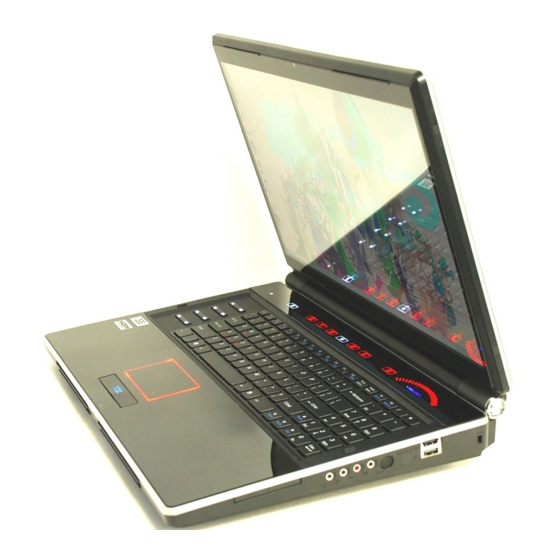
Introduction External Locator - Top View with LCD Panel Open Figure 1 Top View 1. Optional Built-In PC Camera 2. LCD 3. Speakers 4. LED Status Indicators 5. Touch Sensor Instant Keys 6. 8 * Gaming Keys 7. Keyboard 8. TouchPad and Buttons 9. -
Page 17: External Locator - Front & Right Side Views
Introduction External Locator - Front & Right side Views Figure 2 Front Views 1. Speakers 2. LED Power Indicators Figure 3 Right Side Views 1. ExpressCard/54(34) Slot 2. Headphone-In Jack 3. Microphone-In Jack 4. Line-In Jack 5. S/PDIF-Out Jack 6. Combined eSATA/ USB Port 7. -
Page 18: External Locator - Left Side & Rear View
Introduction External Locator - Left Side & Rear View Figure 4 Left Side View 1. DVI-Out Port 2. Powered USB 2.0 Port 3. USB 2.0 Ports 4. RJ-45 LAN Jack 5. HDMI-Out Port 6. Multi-in-1 Card Reader 7. USB 3.0 Ports 8. -
Page 19: External Locator - Bottom View
Introduction External Locator - Bottom View Figure 6 Bottom View 1. Sub Woofer 2. Fan Outlet/Intake 3. Component Bay Cover 4. Battery 5. HDD Bay Overheating To prevent your com- puter from overheating make sure nothing blocks the vent/fan in- takes while the com- puter is in use. -
Page 20: Mainboard Overview - Top (Key Parts)
Introduction Mainboard Overview - Top (Key Parts) Figure 7 Mainboard Top Key Parts 1. KBC-IT8519BX 2. CMOS Battery 3. Mini-Card Connector (WLAN Module) 4. CougarPoint Controller 5. Memory Slots DDR3 So-DIMM 6. Audio Codec ALC892 1 - 8 Mainboard Overview - Top (Key Parts) -
Page 21: Mainboard Overview - Bottom (Key Parts)
Introduction Mainboard Overview - Bottom (Key Parts) Figure 8 Mainboard Bottom Key Parts 1. Memory Slots DDR3 So-DIMM 2. CPU Socket 3. VGA Sockets Mainboard Overview - Bottom (Key Parts) 1 - 9... -
Page 22: Mainboard Overview - Top (Connectors)
Introduction Mainboard Overview - Top (Connectors) Figure 9 Mainboard Top Connectors 1. Touch Sensor Connector 2. MIC Connector 3. LCD Cable Connector 4. LED Cable Connector 5. Subwoofer Connector 6. CCD Cable Connector 7. Power Button Connector 8. Audio Cable Connector 9. -
Page 23: Mainboard Overview - Bottom (Connectors)
Introduction Mainboard Overview - Bottom (Connectors) Figure 10 Mainboard Bottom Connectors 1. Battery Connector 2. DC-In Jack 3. DVI Port 4. USB 2.0 Ports 5. RJ-45 LAN Jack 6. HDMI-Out Port 7. VGA Fan 1 8. VGA Fan 2 9. ODD Connector 10. - Page 24 Introduction 1 - 12...
-
Page 25: Disassembly
Chapter 2: Disassembly Overview This chapter provides step-by-step instructions for disassembling the P180HM series notebook’s parts and subsystems. When it comes to reassembly, reverse the procedures (unless otherwise indicated). We suggest you completely review any procedure before you take the computer apart. -
Page 26: Maintenance Tools
Disassembly NOTE: All disassembly procedures assume that the system is turned OFF, and disconnected from any power supply (the battery is removed too). Maintenance Tools The following tools are recommended when working on the notebook PC: • M3 Philips-head screwdriver •... -
Page 27: Maintenance Precautions
Disassembly Maintenance Precautions The following precautions are a reminder. To avoid personal injury or damage to the computer while performing a re- moval and/or replacement job, take the following precautions: Power Safety Warning 1. Don't drop it. Perform your repairs and/or upgrades on a stable surface. If the computer falls, the case and other Before you undertake components could be damaged. -
Page 28: Disassembly Steps
Disassembly Disassembly Steps The following table lists the disassembly steps, and on which page to find the related information. PLEASE PERFORM THE DISASSEMBLY STEPS IN THE ORDER INDICATED. To remove the Battery: To remove the Wireless LAN Module: 1. Remove the battery page 2 - 5 1. -
Page 29: Removing The Battery
Disassembly Removing the Battery Figure 1 Battery Removal If you are confident in undertaking upgrade procedures yourself, for safety reasons it is best to remove the battery. Slide the latch 1. Turn the computer off, and turn it over. the direction of the ar- Slide the latch in the direction of the arrow. -
Page 30: Removing The Optical (Cd/Dvd) Device
Disassembly Removing the Optical (CD/DVD) Device Figure 2 Optical Device 1. Turn off the computer, and turn it over and remove the battery (page 2 - Removal 2. Locate the component bay cover and remove screws , and remove the bay cover 3. -
Page 31: Removing The Hard Disk Drive
Disassembly Removing the Hard Disk Drive Figure 3 The hard disk drive is mounted in a removable case and can be taken out to accommodate other 2.5" SATA hard disk HDD Assembly drives with a height of 9.5mm (h). Follow your operating system’s installation instructions, and install all necessary driv- Removal ers and utilities (as outlined in Chapter 4 of the User’s Manual) when setting up a new hard disk. - Page 32 Disassembly 4. Remove screws and pull the tab to disconnect the connector from hard disk assembly. Figure 4 5. Lift the hard disk assembly out of the computer. HDD Assembly 6. Remove screws (depending on how many hard disks you have installed in the assembly). Removal (cont’d.) 7.
- Page 33 Disassembly Removing the Hard Disk(s) in the Secondary HDD Bay Figure 5 1. Turn off the computer, and turn it over and remove the battery and r.emove the optical device drive Secondary HDD 2. The secondary hard disk bay is located under the optical device drive. Assembly Removal 3.
-
Page 34: Removing The Keyboard
Disassembly Removing the Keyboard Figure 6 Keyboard 1. Turn off the computer, and turn it over and remove the battery (page 2 - Removal 2. Remove screws & from the bottom of the computer. 3. Turn the computer over, open the Lid/LCD, and carefully (a cable is connected to the underside of the LED cover a. - Page 35 Disassembly 6. Carefully lift the keyboard up, being careful not to bend the keyboard ribbon cable. Figure 7 7. Disconnect the keyboard ribbon cable from the locking collar socket Keyboard Removal 8. Remove the keyboard (cont’d.) e. Disconnect cable from the locking collar.
-
Page 36: Removing The System Memory (Ram) -1
Disassembly Removing the System Memory (RAM) -1 Figure 8 RAM-1 Module The computer has three memory sockets for 204 pin Small Outline Dual In-line Memory Modules (SO-DIMM) DDR III Removal (DDR3) supporting 1066/1333 MHz. The main memory can be expanded up to 8GB. The total memory size is automat- ically detected by the POST routine once you turn on your computer. - Page 37 Disassembly Figure 9 6. Gently pull the two release latches & on the sides of the memory socket in the direction indicated by RAM-1 Module the arrows (Figure Removal (cont’d.) 7. The RAM module will pop-up (Figure e), and you can then remove it. d.
-
Page 38: Removing The System Memory (Ram) - 2
Disassembly Removing the System Memory (RAM) - 2 Figure 10 RAM-2 Module Memory Upgrade Process Removal (cont’d.) 1. Turn off the computer, and turn it over and remove the battery (page 2 - 5) and remove the keyboard (page 2 - 2. -
Page 39: Removing And Installing The Processor
Disassembly Removing and Installing the Processor Figure 11 Processor Removal Processor Removal Procedure 1. Turn off the computer, and turn it over, remove the battery (page 2 - 5), and component bay cover (page 2 - 10). a. Locate the heat sink. 2. - Page 40 Disassembly 5. Turn the release latch towards the unlock symbol , to release the CPU (Figure 12a). 6. Carefully (it may be hot) lift the CPU up out of the socket (Figure 12b). Figure 12 7. See page 2 - 17 for information on inserting a new CPU.
- Page 41 Disassembly Processor Installation Procedure Figure 13 1. Insert the CPU , pay careful attention to the pin alignment, it will fit only one way (DO NOT FORCE IT!), and turn Processor Installation the release latch towards the lock symbol (Figure 13b).
-
Page 42: Removing The Vga Card
Disassembly Removing the VGA Card Figure 14 VGA Card Removal 1. Turn off the computer, and turn it over and remove the battery (page 2 - 5) and component bay cover (page 2 - 2. The VGA card will be visible at point on the mainboard (Figure 16a). -
Page 43: Installing The Vga Card
Disassembly Installing the VGA Card 1. Prepare to fit the VGA card into the slot by holding it at about a 30° angle. Figure 15 2. The card needs to be fully into the slot, and the VGA card and socket have a guide-key and pin which align to allow VGA Card the card to fit securely. -
Page 44: Removing The Wireless Lan Module
Disassembly Removing the Wireless LAN Module Figure 16 Wireless LAN 1. Turn off the computer, and turn it over, remove the battery (page 2 - 5), keyboard and keyboard shielding plate Module Removal (page 2 - 10). 2. The Wireless LAN Module will be visible at point a. -
Page 45: Part Lists
Part Lists Appendix A: Part Lists This appendix breaks down the P180HM series notebook’s construction into a series of illustrations. The component part numbers are indicated in the tables opposite the drawings. Note: This section indicates the manufacturer’s part numbers. Your organization may use a different system, so be sure to cross-check any relevant documentation. -
Page 46: Part List Illustration Location
Part List Illustration Location The following table indicates where to find the appropriate part list illustration. Table A- 1 Part List Illustration Location Parts P180HM Top with Fingerprint page A - 3 Top without Fingerprint page A - 4 Bottom... -
Page 47: Top With Fingerprint
Part Lists Top with Fingerprint Figure A - 1 Top with Fingerprint Top with Fingerprint A - 3... -
Page 48: Top Without Fingerprint
Part Lists Top without Fingerprint Figure A - 2 Top without Fingerprint A - 4 Top without Fingerprint... -
Page 49: Bottom
Part Lists Bottom Figure A - 3 Bottom & Ω Ω 頭厚 信越 Bottom A - 5... -
Page 50: Lcd
Part Lists Figure A - 4 無鉛 (尚盟) 中性 A - 6 LCD... -
Page 51: Mainboard
Part Lists Mainboard Figure A - 5 Mainboard (長騰) Mainboard A - 7... -
Page 52: Dvd
Part Lists Figure A - 6 (志精) A - 8 DVD... -
Page 53: Combo
Part Lists COMBO Figure A - 7 COMBO (志精) COMBO A - 9... - Page 54 Part Lists A - 10...
-
Page 55: Schematic Diagrams
Schematic Diagrams Appendix B: Schematic Diagrams This appendix has circuit diagrams of the P180HM notebook’s PCB’s. The following table indicates where to find the appropriate schematic diagram. Diagram - Page Diagram - Page Diagram - Page Table B - 1... -
Page 56: Sandy Bridge 7/7 Rsvd
Schematic Diagrams System Block Diagram PWR 3.3V/5V/3.3VS/5VS CLEVO P180HM System Block Diagram POWER VCORE Power Button BOARD PWR 1.05VS/1.05VS_VTT CH A SO-DIMM0 CH B SO-DIMM0 CH A SO-DIMM1 CH B SO-DIMM1 TOUCH PAD LED 3 IN 1 Sandy Bridge PWR 0.85VS... - Page 57 Schematic Diagrams Sandy Bridge 1/7 DMI, PEG PEG_R XN[0..7] PEG_RXN [0..7] 13 PEG_R XP[0..7] PEG_RXP[0..7] 13 Sandy Bridge PROCESSOR ( DMI,PEG,FDI ) PEG_TXN[0..7] PEG_TXN[0..7] 13 PEG_TXP[0..7] PEG_TXP[0..7] 13 PEG_R XN[8..15] PEG_RXN [8..15] 14 PEG_R XP[8..15] PEG_RXP[8..15] 14 PEG_TXN[8..15] PEG_TXN[8..15] 14 PEG_TXP[8..15] PEG_TXP[8..15] 14 1.05VS_VTT...
- Page 58 Schematic Diagrams Sandy Bridge 2/7 CLK, MISC Sandy Bridge PROCESSOR ( CLK,MISC,JTAG ) U38B CLK_EXP_P 16 BCLK PROC_SELET DDR3 Compensation Signals PROC_SELET CLK_EXP_N 16 SNB_IVB# BCLK# AN34 1.05VS_VTT SM_RCOMP_0 R108 140_1%_04 SKTOCC# Z0301 R465 1K_04 DPLL_REF_SSCLK Z0302 R464 1K_04 C742 *0.1u_10V_X5R_04 DPLL_REF_SSCLK# H_CATERR#...
- Page 59 Schematic Diagrams Sandy Bridge 3/7 DDR3I Sandy Bridge PROCESSOR ( DDR3 ) U38C U38D M_A_CLK_DDR0 9 M_B_CLK_DDR0 11 M_A_DQ[63:0] SA_CLK[0] 11,12 M_B_DQ[63:0] SB_CLK[0] M_A_CLK_DDR#0 9 M_B_CLK_DDR#0 11 SA_CLK#[0] SB_CLK#[0] M_A_DQ0 M_B_DQ0 M_A_CKE0 9 M_B_CKE0 11 SA_DQ[0] SA_CKE[0] SB_DQ[0] SB_CKE[0] M_A_DQ1 M_B_DQ1 SA_DQ[1] SB_DQ[1]...
- Page 60 Schematic Diagrams Sandy Bridge 4/7 Power PROCESSOR CORE POWER Sandy Bridge PROCESSOR ( POWER ) ICCMAX Maximum Processor XE POWER U38F PROCESSOR UNCORE POWER VCORE 1.05VS_VTT 1.05VS_VTT 8.5A AG35 VCC1 VCORE AG34 AH13 12/04 AG33 VCC2 VCCIO1 AH10 VCC3 VCCIO2 AG32 AG10 C621...
- Page 61 Schematic Diagrams Sandy Bridge 5/7 GFX PWR Sandy Bridge PROCESSOR ( GRAPHICS POWER ) 1.5VS_CPU POWER U38G R137 *0_04 R151 V_SM_VREF Z0601 AT24 AK35 100_04 VAXG1 VAXG_SENSE AT23 AK34 VAXG2 VSSAXG_SENSE AT21 AO3402L VAXG3 AT20 V_SM_VREF_CNT VAXG4 AT18 AT17 VAXG5 R 140 VAXG6 AR24...
- Page 62 Schematic Diagrams Sandy Bridge 6/7 Sandy Bridge Processor 6/7 ( GND ) U38H U38I AT35 AJ22 VSS1 VSS81 AT32 AJ19 VSS2 VSS82 AT29 AJ16 VSS3 VSS83 VSS161 VSS234 AT27 AJ13 VSS4 VSS84 VSS162 VSS235 AT25 AJ10 VSS5 VSS85 VSS163 VSS236 AT22 VSS6 VSS86...
- Page 63 Schematic Diagrams Sandy Bridge 7/7 RSVD Sandy Bridge Processor 7/7 ( RESERVED ) CFG Straps for Processor PEG Static Lane Reversal - CFG2 is for the 16x U38E 1:(Default) Normal Operation; Lane # CFG2 definition matches socket pin map definition RSVD28 0:Lane Reversed RSVD29...
-
Page 64: Ddr3 Cha So-Dimm 0
Schematic Diagrams DDR3 CHA SO-DIMM 0 Channel A SO-DIMM 0 (Button Side) REVERSE TYPE D03 For factory D03 For factory JDIMM1A M_A_A[15:0] M_A_DQ[63:0] 4 M_A_A0 M_A_DQ0 JDIMM1B M_A_A1 M_A_DQ1 M_A_A2 M_A_DQ2 M_A_A3 M_A_DQ3 1.5V M_A_A4 M_A_DQ4 M_A_A5 M_A_DQ5 VDD1 VSS16 M_A_A6 M_A_DQ6 VDD2... - Page 65 Schematic Diagrams DDR3 CHA SO-DIMM 1 Channel A SO-DIMM 1 (Button Side) Sheet 10 of 56 DDR3 CHA SO- DIMM 1 D03 Remove Channel A DIMM1 VTT_MEM 1.5V C218 C248 C214 C234 C244 C211 C213 C224 C725 C738 C730 C720 C728 0.1u_10V_X5R_04 0.1u_10V_X5R_04...
-
Page 66: Ddr3 Chb So-Dimm 0
Schematic Diagrams DDR3 CHB SO-DIMM 0 Channel B SO-DIMM 0 (Bottom Side) REVERSE TYPE JDIMM2A 4,12 M_B_A[15:0] M_B_DQ[63:0] 4,12 M_B_A0 M_B_DQ0 JDIMM2B M_B_A1 M_B_DQ1 M_B_A2 M_B_DQ2 M_B_A3 M_B_DQ3 1.5V M_B_A4 M_B_DQ4 D02 CHANGE TO BOTTOM SIDE M_B_A5 M_B_DQ5 VDD1 VSS16 M_B_A6 M_B_DQ6 VDD2... - Page 67 Schematic Diagrams DDR3 CHB SO-DIMM 1 Channel B SO-DIMM 1 (Top Side) D03 For factory REVERSE TYPE D03 For factory JDIMM3A 4,11 M_B_A[15:0] M_B_D Q[63:0] 4,11 M_B_A0 M_B_D Q0 JDIMM3B M_B_A1 M_B_D Q1 M_B_A2 M_B_D Q2 M_B_A3 M_B_D Q3 1.5V M_B_A4 M_B_D Q4 M_B_A5...
-
Page 68: Mxm 3.0 Master
Schematic Diagrams MXM 3.0 MASTER MXM 3.0 SMD_THERM_2 R437 *2.2K_04 3.3VS SMC_THERM_2 R438 *2.2K_04 VIN_MXM VIN_MXM J_MXM2A MASTER Pull high to VDD3 in KBC side 14,19 PEG_RST# E1-1 E2-1 PWR_SRC PWR_SRC J_MXM2B E1-2 E2-2 E1-3 PWR_SRC PWR_SRC E2-3 PWR_SRC PWR_SRC CLK_PCIE_MXM1# PEX_REFCLK# CLK_REQ#... -
Page 69: Mxm 3.0 Slave
Schematic Diagrams MXM 3.0 SLAVE MXM 3.0 MEP4435Q8 VIN_MXM VIN_MXM 3.3VS 3VRUN VIN_MXM J_MXM1A 0_06 E1-1 E2-1 SLAVE PWR_SRC PWR_SRC E1-2 E2-2 C567 R429 R430 PWR_SRC PWR_SRC E1-3 E2-3 C579 *0.01u_50V_X7R_04 E1-4 PWR_SRC PWR_SRC E2-4 Z1417 *22_04 100K_04 PWR_SRC PWR_SRC E1-5 E2-5 PWR_SRC(10A)--7-20V... -
Page 70: Cpt 1/9 Hda, Sata
Schematic Diagrams CPT 1/9 HDA, SATA INTVRMEN- Integrated SUS 1.05V VRM Enable CougarPoint - M (HDA,JTAG,SATA) High - Enable Internal VRs Low - Enable External VRs D01A 01/04 Change to SOT-23 RTCVCC 2 0 mils C308 2 0 mils VDD3 15p_50V_NPO_04 Zo= 50O? 5% C191... -
Page 71: Cpt 2/9 Pcie, Smbus
Schematic Diagrams CPT 2/9 PCIE, SMBUS CougarPoint - M (PCI-E,SMBUS,CLK) 3.3V Zdiff= 85O U14B SMBus Zo= 50O SMB_CLK_DDR3 R520 2.2K_04 BG34 SMB_DATA_DDR3 R188 2.2K_04 PCIE_RXN1_WLAN PERN1 BJ34 PCH_BT_EN# PCIE_RXP1_WLAN PCH_BT_EN# 28,31 PERP1 SMBALERT# / GPIO11 C306 0.1u_10V_X7R_04 PCIE_TXN1_C AV32 SML0_CLK R184 2.2K_04 PCIE_TXN1_WLAN... -
Page 72: Cpt 3/9 Dmi, Pwrgd
Schematic Diagrams CPT 3/9 DMI, PWRGD CougarPoint - M (DMI,FDI,GPIO) U14C BC24 BJ14 DMI_RXN0 DMI0RXN FDI_RXN0 BE20 AY 14 DMI_RXN1 DMI1RXN FDI_RXN1 BG18 BE14 DMI_RXN2 DMI2RXN FDI_RXN2 BG20 BH13 DMI_RXN3 DMI3RXN FDI_RXN3 BC12 FDI_RXN4 BE24 BJ12 DMI_RXP0 DMI0RXP FDI_RXN5 BC20 BG10 DMI_RXP1 DMI1RXP... -
Page 73: Cpt 4/9 Lvds, Ddi, 9/9 Gnd
Schematic Diagrams CPT 4/9 LVDS, DDI, 9/9 GND CougarPoint - M (LVDS,DDI) CougarPoint - M (GND) U14I U14H VSS[159] VSS[259] VSS[0] AY 42 VSS[160] VSS[260] AY 46 AA17 AK38 VSS[161] VSS[261] VSS[1] VSS[80] VSS[162] VSS[262] VSS[2] VSS[81] AK42 VSS[163] VSS[263] VSS[3] VSS[82] AA33... -
Page 74: Cpt 5/9 Pci, Usb
Schematic Diagrams CPT 5/9 PCI, USB CougarPoint - M (PCI,USB) U14E AY 7 Boot BIOS Strap RSVD1 RSVD2 BG26 RSVD3 BJ26 BBS_BIT1 BBS_BIT0 Boot BIOS Location RSVD4 BH25 BJ16 AT10 BG16 RSVD5 AH38 RSVD6 Reserved (NAND) AH37 RSVD7 AK43 PCI (Desktop only) RSVD8 AK45 PLT_RST# Buffer... -
Page 75: Cpt 6/9 Gpio, Cpu
Schematic Diagrams CPT 6/9 GPIO, CPU CougarPoint - M (GPIO,VSS_NCTF,RSVD) U14F S_GPIO BMBUSY # / GPIO0 TACH 4 / GPIO68 SATA_OD D_PWRGT 28 SMI# PC H_GPIO69 R282 1.5K_1%_04 SMI# TACH1 / GPIO1 TACH 5 / GPIO69 DGPU HDP (NV CONTROL BYSELF) DGPU_H PD_INTR# PC H_GPIO70 R279... -
Page 76: Cpt 7/9 Pwr
Schematic Diagrams CPT 7/9 PWR CougarPoint - M (POWER) 3.3VS R316 0_06 POWER SUSB 3,38,41,43,44 U14G 1.05VS VCCA_DAC_3.3VS HCB1608KF-121T25 1.14A AA23 Z2102 VCCCORE[1] VCCADAC AC23 VCCCORE[2] AD21 C170 C704 C696 C698 C348 C351 C377 C385 C387 R312 VCCCORE[3] AD23 C367 VCCCORE[4] VSSADAC SHDN#... -
Page 77: Cpt 8/9 Pwr
Schematic Diagrams CPT 8/9 PWR This pin can be left as no connect in External Graphics CougarPoint - M (POWER) On-Die VR ena bled mode Voltage Rail Voltage S0 Iccmax Current (A) 1.05VS 1.05VS R277 *0_04 POWER V_PROC_IO 1.05 0.001 U14J 3.3V V5REF... -
Page 78: Sata Hdd Conn, Re- Driver
Schematic Diagrams SATA HDD CONN, Re- Driver SINGAL SATA HDD 3.3VS R421 Note: SATA Gen2 Closed TO U41 4.7K_04 SN75LVCP412 C550 0.01u_16V_X7R_04 Z2303 SATA_TXP4 IZ01 SATA_TXP4 SATA_TXN4 IZ02 SATA_TXP4_R SATA_TXN4 RX_0P TX_0P SATA_TXP4_R 36 SATA_TXN4_R SN75LVCP601RTJ Re-Driver. SATA_TXN4_R 36 RX_0N TX_0N C549 0.01u_16V_X7R_04... - Page 79 Schematic Diagrams CPT, DVI CRT/DVI Connector Close to connector VGA_R FCM1005MF-600T01 Z2401 FCM1005MF-600T01 FRED VGA_R VGA_G Z2402 FGRN Z2408 FCM1005MF-600T01 FCM1005MF-600T01 C136 5p_50V_NPO_04 VGA_G DVI_D#2 EX_DVI_DATA2#_R C137 0.1u_16V_Y5V_04 VGA_B FCM1005MF-600T01 Z2403 FCM1005MF-600T01 FBLUE Z2409 C133 0.1u_16V_Y5V_04 EX_DVI_DATA2_R VGA_B DVI_D2 C132 5p_50V_NPO_04 *WCM2012F2S-161T03-SHORT Z2410...
-
Page 80: Led Panel
Schematic Diagrams LED PANEL 18.4" PANEL 2.2K_04 3.3VS 2.2K_04 J_LCD1 BRIGHTNESS LVDS_DDC_DAT 13 LVDS_UCLKN LVDS_DDC_CLK 13 LVDS_UCLKP LVDS_U2N 13 LVDS_U1N LVDS_U2P 13 *BAV99N3 LVDS_U1P LVDS_U0N 13 3.3V LVDS_LCLKN LVDS_U0P 13 LVDS_LCLKP LVDS_L2N 13 LVDS_L1N LVDS_L2P 13 LVDS_L1P *0.1u_16V_Y 5V_04 3.3VS LVDS_L0N PLVDD LVDS_L0P... -
Page 81: Fan Control
Schematic Diagrams FAN CONTROL Touch Sensor LED control FAN CONTROL 5VS_JTS *0_06 VOUT CPU FAN Z3131 10K_04 7.5K_1%_04 APL5317-12BI-TRG Z2601 LED_SET VOUT 0.1u_16V_Y5V_04 1u_10V_Y 5V_06 CPU_FAN VSET Vo=0.8*(1+R1/R2) C375 C378 G990P11U 2.2K_1%_04 0.1u_16V_Y 5V_04 *10u_10V_Y5V_08 5VS_CPUFAN J_CPUFAN1 R582 4.7K_04 C386 3.3VS 3.9K_04 10u_6.3V_X5R_08... -
Page 82: Hdmi, Rj45 Conn
Schematic Diagrams HDMI, RJ45 CONN HDMI Connector *WCM2012F2S-161T03-SHORT HDMI_CLK HDMI_CCLK_C C709 0.1u_10V_X7R_04 HDMI_CCLK 13 HDMI_CLK# HDMI_CCLK#_C C705 0.1u_10V_X7R_04 HDMI_CCLK# 13 *WCM2012F2S-161T03-SHORT HDMI_2 HDMI_C2_C C724 0.1u_10V_X7R_04 HDMI_C2 13 HDMI_#2 HDMI_C#2_C R539 1_04 R560 1_04 C721 0.1u_10V_X7R_04 HDMI_C#2 13 *WCM2012F2S-161T03-SHORT 5VS_HDMI_R HDMI_1 HDMI_C1_C C718 0.1u_10V_X7R_04... -
Page 83: Odd, Ccd, Usb 2.0, Bt, Tpm
Schematic Diagrams ODD, CCD, USB 2.0, BT, TPM SATA ODD D03 For PDA J_ODD1 5V_CCD SATA_TXP2_C C391 0.01u_16V_X7R_04 R243 0.2_06 R255 0.2_06 SATA_TXP2 15 SATA_TXN2_C C402 0.01u_16V_X7R_04 SATA_TXN2 15 VOUT SATA_RXN2_C C427 0.01u_16V_X7R_04 SATA_RXN2 15 SATA_RXP2_C C434 0.01u_16V_X7R_04 SATA_RXP2 15 C582 C583 CCD_EN... -
Page 84: Codec, Dmic
Schematic Diagrams CODEC, DMIC DIGITAL *HCB1005KF-121T20 3.3VS_DMIC 3.3VS_AUD 5VS_AUD 0_04 3.3VS 3.3VS 40mil 40mil MTP3403N3 C397 C418 C479 10u_10V_Y 5V_08 10u_10V_Y5V_08 6-20-43130-104 *0.1u_16V_Y5V_04 3.3V AUDG AUDG 3.3VS_DMIC Z2903 R381 100K_04 J_DMIC1 47p_50V_NPO_04 VREF_CODEC D01A 01/06 Z2901 FCM1005KF-121T03 DMIC_CLK C407 0.1u_16V_Y5V_04 Z2902 DMIC_DATA DMIC_CLK... -
Page 85: Audio Amp, Spk
Schematic Diagrams AUDIO AMP, SPK FRONT R/L 4ohm D03 For Audio issue 5VS_AMP HCB1005KF-121T20 12MIL D03A 6/13 R321 *5.1K_1%_04 C456 C440 C433 FCM1005KF-121T03 AUDG SPKOUTL+_C SPKOUTL+_R FRONT_L R347 11K_1%_04 Z3001 C441 0.01u_16V_X7R_04 Z3005 0.1u_16V_Y5V_04 1u_10V_Y5V_06 10u_10V_Y5V_08 SPKOUTL-_C SPKOUTL-_R SPKOUTL-_R 6-20-53140-106 FRONT_L LIN- PVDD... -
Page 86: Wlan, Tv, Charger Usb
Schematic Diagrams WLAN, TV, Charger USB MINI-PCIE CARD (WLAN + 80 PORT+ COMBO) MINI-PCIE CARD For TV 3.3VS 1.5VS is for MC770AQ TV CARD 20 mil 3.3V C143 C315 C200 C206 D03 Remove TV Card component 0.1u_16V_Y 5V_04 J_MINI1 *0.1u_16V_Y5V_04 *0.1u_16V_Y5V_04 *10u_10V_Y5V_08 Z3101... -
Page 87: Lan, Card Reader
Schematic Diagrams LAN, Card Reader SD_CLK VDD3 3.3V_LAN JMC251 C C439 near Pin#41 R218 0_06 Switching Regulator ISON close to PIN33 *10p_50V_NPO_06 R163 *4.7K_04 R215 *100K_1%_04 DVDD 3.3VS SD_CLK R214 0_04 (>20mil) LAN_SCL R164 *4.7K_04 REGLX DVDD R173 *4.7K_04 SD_CD# (>20mil) SDXC_POWER SWF2520CF-4R7M-M... -
Page 88: Ieee 1394
Schematic Diagrams IEEE 1394 JMB380C XTAL: 6-22-24R57-1B4 1394_XI C372 20p_50V_NPO_04 Note: Close to JMB380 Zdiff= 110O R302 *24.576MH z C360 220p_50V_NPO_04 1M_04 R283 4.99K_1%_04 R287 56_04 1394_XO C373 20p_50V_NPO_04 Z3301 R284 56_04 Note: Close to JMB380 1394_TPB0- 1394_TPB0+ 1394_TPA0- 1394_TPA0+ Sheet 33 of 56 3.3VS_CAR D 3.3VS... - Page 89 Schematic Diagrams USB 3.0 3.3V 1.05V_USB 3.3VA 1ST: 6-04-25512-B71 3.3V 3.3V D01B PDA X7R=>Y5V 2ND: 6-04-25512-B72 C450 C413 C414 3RD: 6-04-25010-A91 C409 HCB1608KF-121T25 3.3V 0.1u_16V_Y5V_04 0.1u_16V_Y 5V_04 0.1u_16V_Y 5V_04 0.1u_16V_Y 5V_04 *NC_04 512Kbit KBC_SPI_*_R = 0.1"~0.5" R404 C504 0.1u_16V_Y 5V_04 R379 3.3VA USB_SPI_VDD...
-
Page 90: Kbc Ite It8519-Bx
Schematic Diagrams KBC ITE IT8519-BX KBC_AVDD HCB1005KF-121T20 VDD3 C328 R237 10K_04 MODEL_ID VDD5 VDD3 VDD3 C747 C384 C361 C349 C330 C329 C316 R247 *10K_04 0.1u_16V_Y 5V_04 10u_10V_Y5V_08 0.1u_16V_Y5V_04 0.1u_16V_Y 5V_04 0.1u_16V_Y5V_04 *0.1u_16V_Y5V_04 *0.1u_16V_Y 5V_04 CIR_RX C380 VDD3 BAV99N3 HCB1005KF-121T20 0.1u_16V_Y5V_04 KBC_AGND EC_VCC 3.3VS... -
Page 91: Small Board Conn-A
Schematic Diagrams SMALL BOARD CONN-A AUDIO B'd GAME KEY B'd Click B'd H=1.8 5VS_JTP J_TP1 *56mil_08 TP_DATA TP_DATA 35 TP_CLK TP_CLK LED_ACIN 35 10/28 EC high active LED_PWR 35 J_MB1 LED_BAT_CHG 35 SATA_RXP3 H=1.8 SATA_RXP3 VCCUSB_01 LED_BAT_FULL 35 SATA_RXN3 SATA_RXN3 3.3VS_JGAMEKEY 3.3VS SATA_TXN3... -
Page 92: Small Board Conn-B
Schematic Diagrams SMALL BOARD CONN-B TOUCH SENSOR B'd TOUCH PAD LED B'd LOGO LED B'd H=1.8 *56mil_08 5VS_JTS 5VS_JSENSOR J_TLED1 J_CLED1 *56mil_08 3.3VS 3.3VS_JSENSOR J_SENSOR1 10 mils 5VS_TLED 5VS_JCLED R297 0_06 *56mil_08 5VS_TLED 5VS_JSENSOR 5VS_BL VDD3 VDD3_JSENSOR CLED_R LLED_R CLED_G 0_06 LLED_G 0_06... -
Page 93: Power System
Schematic Diagrams POWER SYSTEM POWER SW SY S5V SY S5V R557 R265 10K_04 10K_04 SUSB 3,21,41,43,44 DD_ON# 28,31,43 MTN7002ZHS3 MTN7002ZHS3 PC173 PC172 PJ16 17,29,34,35,37 SUSB# 31,35 D D_ON *OPEN-1mm *0.1u_16V_Y 5V_04 *OPEN -1mm *0.1u_16V_Y 5V_04 R570 R613 D03 For PDA D03 For PDA 100K_04 100K_04... -
Page 94: Pwr Vcore-1
Schematic Diagrams PWR VCORE-1 Z3916 Z3901 IMON PR103 10_04 PC77 680p_50V_X7R_04 VCORE_1 PR104 1.21K_1%_04 B~4350 PUT COLSE PR81 PC66 PR102 24.9k_1%_04 PC76 TO VCORE 13.7K_1%_0402 5600p_50V_X7R_04 0.1u_10V_X5R_04 Phase 1 A_GND Inductor PC70 100K_NTC_06_B Quad 45W CPU Z3902 100p_50V_NPO_04 PC68 22p_50V_NPO_04 VID1=0.9V A_GND A_GND... -
Page 95: Pwr Vcore-2
Schematic Diagrams PWR VCORE-2 VCORE_2 PC139 PC51 PC46 PC42 D03 POWER Z4003 PR58 2.2_06 PC50 0.22u_10V_X7R_06 PQ40 PQ46 *IRFH7914PBF/ NTMFS4926N IR FH7914PBF/ NTMFS4926N D03 EMI NCP5911 D03 EMI VCORE Z4001 VREG_SW1_HG VREG_SW1_HG_R PR187 0_04 PL12 VREG_SW1_OUT VCORE VR1_PWM1 PQ45 PQ39 Z4002 PR61 IRFH 7932/ NTMFS4935N... -
Page 96: Pwr 1.05Vs/ 1.05Vs Cpu
Schematic Diagrams PWR 1.05VS/ 1.05VS CPU PD12 PR25 1.05V_ON RB0540S2 PC14 PC13 PC110 PC111 PC109 PC187 D03 For POWER 100K_1%_04 Z4104 PR24 9.1K_1%_04 SUSB MTN7002ZHS3 3,21,38,43,44 SUSB UP6127 PQ32 PC17 Z4107 QM3002S *0.1u_16V_Y 5V_04 PC10 1.05VS 0.1u_50V_Y 5V_06 V1.05 PJ13 1.05VS PR28 10K_04... -
Page 97: Pwr 0.85Vs
Schematic Diagrams PWR 0.85VS PC 95 PR 127 0. 022u_16V_X7R_04 10K_04 0.9V 0.8V 0.7V 0.6V 0.85VS_PWR GD 17 VCCSA_VID0 VCCSA_VID1 PR116 0_04 Z4201 9.31K_1%_04 PR115 9.31K_1%_04 PD 1 Z4202 RB0540S2 12K_1%_04 PR114 10K_1%_04 PR 119 Z4215 100_04 Z4203 Z4216 Sheet 42 of 56 10K_1%_04 PR113 10K_1%_04... -
Page 98: Pwr 1.5V/ Vtt Mem
Schematic Diagrams PWR 1.5V/ VTT MEM D03 POWER PC21 PC23 PC24 PC22 VDDQ uP6163 RB0540S2 PC16 D03 EMI VTT_MEM 10u_10V_Y5V_08 1.5V PC104 0.1u_10V_X5R_04 PQ33 Z4309 VLDOIN VBST IRFH7914PBF/ NTMFS4926N VDDQ PR27 Z4301 Z4310 Z4316 VTT_MEM DRVH D01B 02/21 PJ 15 2.2_1%_06 *OPEN_2A 1.0UH_10*10*4.5... -
Page 99: Pwr 1.8Vs/ 1.5Vs/ 1.5Vs Cpu
Schematic Diagrams PWR 1.8VS/ 1.5VS/ 1.5VS CPU 1.8VS 1.5VS NM OS ? ? ? ? PIN6? PQ14A V1.8 1.8VS SYS15V 1.5VS 1.5V MTNN20N03Q8 3.3V PC31 R101 2.2u_6.3V_Y5V_06 *OPEN_2A 1M_04 PR38 10K_04 C187 C197 3.3V VCNTL 1.8VS_PWRGD *10mil_short Z4401 1.5VS_EN 0.1u_16V_Y5V_04 100_04 1.8VS_PWRGD VOUT... -
Page 100: Pwr Vdd3/ Vdd5
Schematic Diagrams PWR VDD3/ VDD5 VREF PR173 *0_04 PR165 0_04 PC150 1u_10V_Y 5V_06 PR172 PR171 EN_3V EN_5V PC151 100K_04 100K_04 PC152 1000p_50V_X7R_04 1000p_50V_X7R_04 PU10 VREG3 PC87 PC86 PC155 PR175 *10K_04 Z4508 4.7u_25V_X5R_08 4.7u_25V_X5R_08 VDD3 SYS5V VDD5 LDO3 1u_6.3V_X5R_06 PC158 PC159 PC85 PC157 PC160... -
Page 101: Pwr Charger, Dc In
Schematic Diagrams PWR CHARGER, DC IN Z4606 Charge Current : 2.8A Charge Voltage 16.8V Total Power : 200W PQ22 P2003EVG PR108 0_04 PQ28 ME4425 D03 POWER PQ21 P2003EVG PR19 PR101 HCB4532K-800_18 0.01_1%_32 470K_04 Z4602 6-20-B3H10-103 ? ? JBATTA1 D01B 02/21 PQ19A PR13 PD1503YVS... -
Page 102: Screw Hole
Schematic Diagrams SCREW HOLE H7_0D3_7 H7_0D3_7 H7_0D3_7 H7_0D3_7 H7_0D3_7 H7_0D3_7 H7_0D3_7 H7_0D3_7 H7_0D3_7 H7_0D3_7 C315D110 C315D110 C315D110 C315D110 C315D110 C315D110 C315D110 C315D110 C315D110 C315D110 C315D110 C315D110 C315D110 Sheet 47 of 56 CT276D110 CT276D110 SCREW HOLE C276D165 C276D165 C276D165 C276D165 12/10 H7_0D3_7 H7_0D3_7 C315D165... -
Page 103: Express Card Board
Schematic Diagrams EXPRESS CARD BOARD EXPRESS CARD E3.3V EC371 0.1u_16V_Y5V_04 E3.3V GND_E EBUF_PLT_RST# 74AHC1G08GW E1.5VS E3.3VS E3.3VS E3.3V ER173 ER171 EC261 EC263 EC262 GND_E E1.5VS E3.3VS E3.3V *100K_04 *100K_04 EJ_NEW1 36mils ENC_3.3VAUX GND_E AUXIN AUXOUT +3.3VAUX 48mils ENC_3.3V 3.3VIN 3.3VOUT +3.3V +3.3V GND_E... -
Page 104: Isdb-T Card/ Tv Card
Schematic Diagrams ISDB-T CARD/ TV CARD ISDB-T CARD/ TV CARD D01B 0119 Add 1.5VS for 3G MINI CARD to support MC770AQ 3G POWER EUIM_VPP EVDD3 E3.3V E3G_3.3V ER544 *0_04 EQ31 >120 mil *AO3415 >120mil EC388 *150u_6.3V_V_A GND_E Need check if use A360 ISDB-T Wake up EC610 *0.1u_16V_Y 5V_04 EC767... -
Page 105: Audio Board
Schematic Diagrams AUDIO BOARD AUDIO BOARD A3.3VS USB + eSATA Combo Connector AJ_MB1 AeSATA_RXP AR11 Note: D03 choke change to short pad AVCCUSB1 AeSATA_RXN Closed TO AU1 4.7K_04 AeSATA_TXN SN75LVCP412 AeSATA_TXP_C 0.01u_16V_X7R_04 AZ25 AZ26 AeSATA_TXP AUSB_PP6 AC21 AZ5007 AUSB_PN6 0.01u_16V_X7R_04 AeSATA_TXN_C 0.01u_16V_X7R_04 AZ27... -
Page 106: Power Button Board
Schematic Diagrams POWER BUTTON BOARD POWER BUTTON B'D B3.3VS Sheet 51 of 56 B3.3VS 6-53-3150B-245 POWER BUTTON 220_04 BSW1 BJ_MB1 0.1u_16V_Y5V_04 TJG-533-S-T/R BOARD BM_BTN# BGND 6-52-57301-020 BM_BTN# 88266-03001 6-20-63130-103 RY -SP150DBW71-5A BGND 11/30 White LED BGND BH_1 mth5_0d2_5 BGND B - 52 POWER BUTTON BOARD... -
Page 107: Click & Fp Board
Schematic Diagrams CLICK & FP BOARD CLICK BOARD LIFT 6-53-3150B-245 BAT CHARGER LED POWER ON LED CSW1 TJG-533-S-T/R 0.1U_16V_Y 5V_04 C5VS CTPBUTTON_L 10/28 EC high active CGND CJ_MB1 CJ_TP1 C5VS CTP_DATA CTP_CLK CTP_DATA CTP_CLK 220_04 220_04 220_04 220_04 CGND CLED_ACIN CGND CGND CLED_PWR... -
Page 108: Game Key Board
Schematic Diagrams GAME KEY BOARD GAME KEY BOARD 11/30 White LED 6-53-3150B-245 6-53-3150B-245 GSW2 GSW5 6-52-57301-020 TJG-533-S-T/R TJG-533-S-T/R GGAME#1 GGAME#5 G3.3VS G3.3VS G3.3VS G3.3VS 0.1u_16V_Y5V_04 0.1u_16V_Y5V_04 220_04 220_04 220_04 220_04 G_GND GSW1 G_GND GSW6 GZ5301 GZ5302 GZ5303 GZ5304 TJG-533-S-T/R TJG-533-S-T/R GGAME#2 GGAME#6 RY-SP150DBW71-5A... -
Page 109: Cir Board
Schematic Diagrams CIR BOARD CIR BOARD KH_O1 KH_O2 KH_O3 Sheet 54 of 56 KGND KGND CIR BOARD KVDD5 KJ_MB1 KCIR_RX KVDD5 *88266-03001 KGND *IRM-V038/TR1-P 6-20-63130-103 KVDD5_CIR *100_04 GND2 GND2 GND1 GND1 *0.1u_16V_Y5V_04 *4.7u_10V_X5R_06 *10u_10V_Y5V_08 KGND KGND KGND KCIR_RX D03 Uninstall CIR component CIR BOARD B - 55... - Page 110 Schematic Diagrams FINGER BOARD FUSB_CONN USB_CONNECT FBDRIVE1 BDRIVE1 FBDRIVE2 BDRIVE2 FBEZEL1 BEZEL1A The TESD_GND trace has to be wide (> 20mil) BEZEL1B The path be marked in FBEZEL2 BEZEL2A needs to be design to be short and at low impedance. BEZEL2B FREG_OUT REG_OUT...
- Page 111 Schematic Diagrams POWER ON SEQUENCE P180HM D01 EVT POWER ON SEQUENCE PWR_SW# PWR_SW# DD_ON 43ms DD_ON 1.54ms 3.3V 3.3V 1.268ms RSMRST# 229.8ms RSMRST# PWR_BTN# 204ms 56ms PWR_BTN# 332.4ms SUSC# SUSC# 1.5V 1.74ms 1.74ms Sheet 56 of 56 1.5VS_CPU POWER ON...
- Page 112 Schematic Diagrams B - 58...
Need help?
Do you have a question about the P180HM and is the answer not in the manual?
Questions and answers