Table of Contents
Advertisement
Quick Links
Advertisement
Table of Contents

Subscribe to Our Youtube Channel
Related Manuals for EUROCOM P150HM


Summary of Contents for EUROCOM P150HM
- Page 1 P150HM SERVICE MANUAL...
- Page 3 Preface Notebook Computer P150HM Service Manual...
- Page 4 Preface Notice The company reserves the right to revise this publication or to change its contents without notice. Information contained herein is for reference only and does not constitute a commitment on the part of the manufacturer or any subsequent ven- dor.
- Page 5 Preface About this Manual This manual is intended for service personnel who have completed sufficient training to undertake the maintenance and inspection of personal computers. It is organized to allow you to look up basic information for servicing and/or upgrading components of the P150HM series notebook PC.
- Page 6 Preface IMPORTANT SAFETY INSTRUCTIONS Follow basic safety precautions, including those listed below, to reduce the risk of fire, electric shock and injury to per- sons when using any electrical equipment: 1. Do not use this product near water, for example near a bath tub, wash bowl, kitchen sink or laundry tub, in a wet basement or near a swimming pool.
-
Page 7: Instructions For Care And Operation
Preface Instructions for Care and Operation The notebook computer is quite rugged, but it can be damaged. To prevent this, follow these suggestions: Don’t drop it, or expose it to shock. If the computer falls, the case and the components could be damaged. Do not expose the computer Do not place it on an unstable Do not place anything heavy... -
Page 8: Power Safety
Preface Avoid interference. Keep the computer away from high capacity transformers, electric motors, and other strong mag- netic fields. These can hinder proper performance and damage your data. Take care when using peripheral devices. Use only approved brands of Unplug the power cord before peripherals. -
Page 9: Battery Precautions
Preface Battery Precautions • Only use batteries designed for this computer. The wrong battery type may explode, leak or damage the computer. • Do not continue to use a battery that has been dropped, or that appears damaged (e.g. bent or twisted) in any way. Even if the computer continues to work with a damaged battery in place, it may cause circuit damage, which may possibly result in fire. -
Page 10: System Startup
Preface Related Documents You may also need to consult the following manual for additional information: User’s Manual on Disc This describes the notebook PC’s features and the procedures for operating the computer and its ROM-based setup pro- gram. It also describes the installation and operation of the utility programs provided with the notebook PC. System Startup 1. -
Page 11: Table Of Contents
Preface Contents Introduction ..........1-1 Top with Fingerprint ..............A-3 Top without Fingerprint ..............A-4 Overview ..................1-1 Bottom ................... A-5 External Locator - Top View with LCD Panel Open ......1-4 LCD ....................A-6 External Locator - Front & Right side Views .........1-5 COMBO .................. - Page 12 Preface CougarPoint - M 6/9 ..............B-24 X7100 Click Board ...............B-56 CougarPoint - M 7/9 ..............B-25 X7100 Fingerprint Board ..............B-57 CougarPoint - M 8/9 ..............B-26 TPM ....................B-58 CougarPoint - M 9/9 ..............B-27 X5100 HDD Board ...............B-59 3G, CCD ..................B-28 Updating the FLASH ROM BIOS..
-
Page 13: Introduction
Introduction Chapter 1: Introduction Overview This manual covers the information you need to service or upgrade the P150HM series notebook computer. Information about operating the computer (e.g. getting started, and the Setup utility) is in the User’s Manual. Information about driv- ers (e.g. -
Page 14: Specifications
Introduction Specifications Processor Options Video Adapter Intel® Core™ i7 Processor Extreme Edition nVIDIA® GeForce GTX 485M PCIe Video Card i7-2920XM (2.50GHz) 2GB GDDR5 Video RAM on board 8MB L3 Cache, 32nm, DDR3-1600MHz, TDP 55W Microsoft DirectX® 11 Compatible Intel® Core™ i7 Processor nVIDIA®... -
Page 15: Overview
Introduction Interface Two USB 3.0 Ports Two USB 2.0 Ports (Note one USB 2.0 port can supply power when the system is off but still powered by the AC/DC adapter) One eSATA & USB 2.0 Combo Port One HDMI-Out Port One DVI-Out Port One IEEE1394a Port One S/PDIF-Out Jack... -
Page 16: External Locator - Top View With Lcd Panel Open
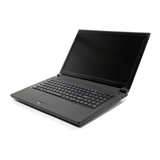
Introduction External Locator - Top View with LCD Panel Open Figure 1 Top View 1. PC Camera 2. LCD 3. LED Status Indicators 4. Power Button 5. Speakers 6. Keyboard 7. Built-In Microphone 15.6” (39.62cm) 8. TouchPad and Buttons 9. Fingerprint Reader (Optional) 1 - 4 External Locator - Top View with LCD Panel Open... -
Page 17: External Locator - Front & Right Side Views
Introduction External Locator - Front & Right side Views Figure 2 Front Views 1. LED Power Indicators Front Figure 3 Right Side Views 1. Optical Device Drive Bay 2. Emergency Eject Right Hole 3. Headphone Jack 4. Microphone Jack 5. S/PDIF-Out Jack 6. -
Page 18: External Locator - Left Side & Rear View
Introduction External Locator - Left Side & Rear View Figure 4 Left Side View 1. RJ-45 LAN Jack 2. USB 3.0 Ports 3. USB 2.0 Port 4. Mini-IEEE 1394a Left Port 5. Multi-in-1 Card Reader Figure 5 Rear View 1. Vent 2. -
Page 19: External Locator - Bottom View
Introduction External Locator - Bottom View Figure 6 Bottom View 1. Vent 2. Component Bay Cover 3. Sub Woofer 4. HDD Bay 5. Battery Overheating To prevent your com- puter from overheating make sure nothing blocks the vent/fan in- takes while the com- puter is in use. -
Page 20: Mainboard Overview - Top (Key Parts)
Introduction Mainboard Overview - Top (Key Parts) Figure 7 Mainboard Top Key Parts 1. Platform Controller Hub 2. Audio Codec 3. KBC ITE IT8519E 1 - 8 Mainboard Overview - Top (Key Parts) -
Page 21: Mainboard Overview - Bottom (Key Parts)
Introduction Mainboard Overview - Bottom (Key Parts) Figure 8 Mainboard Bottom Key Parts 1. VGA-Card Connector 2. CPU Socket (no CPU installed) 3. Memory Slots DDR3 SO-DIMM (Primary) 4. Hard Disk Connector 5. Mini-Card Connector (3G Module) 6. JMC 251C Mainboard Overview - Bottom (Key Parts) 1 - 9... -
Page 22: Mainboard Overview - Top (Connectors)
Introduction Mainboard Overview - Top (Connectors) Figure 9 Mainboard Top Connectors 1. CCD Connector 2. USB 2.0 Port 3. Mini-IEEE 1394a Port 4. Multi-in-1 Card Reader 5. USIM Card 6. LED 2 Cable Connector 7. Keyboard Cable Connector 8. TouchPad Cable Connector 9. -
Page 23: Mainboard Overview - Bottom (Connectors)
Introduction Mainboard Overview - Bottom (Connectors) Figure 10 Mainboard Bottom Connectors 1. DC-In Jack 2. DVI-Out Port 3. HDMI-Out Port 4. eSATA/USB 2.0 Combo Port 5. VGA Fan Cable Connector 6. Sub Woofer Cable Connector 7. CPU Fan Cable Connector 8. - Page 24 Introduction 1 - 12...
-
Page 25: Disassembly
Disassembly Chapter 2: Disassembly Overview This chapter provides step-by-step instructions for disassembling the P150HM series notebook’s parts and subsystems. When it comes to reassembly, reverse the procedures (unless otherwise indicated). We suggest you completely review any procedure before you take the computer apart. Procedures such as upgrading/replacing the RAM, optical device and hard disk are included in the User’s Manual but are repeated here for your convenience. -
Page 26: Maintenance Tools
Disassembly NOTE: All disassembly procedures assume that the system is turned OFF, and disconnected from any power supply (the battery is removed too). Maintenance Tools The following tools are recommended when working on the notebook PC: • M3 Philips-head screwdriver •... -
Page 27: Maintenance Precautions
Disassembly Maintenance Precautions The following precautions are a reminder. To avoid personal injury or damage to the computer while performing a re- moval and/or replacement job, take the following precautions: Power Safety Warning 1. Don't drop it. Perform your repairs and/or upgrades on a stable surface. If the computer falls, the case and other Before you undertake components could be damaged. -
Page 28: Disassembly Steps
Disassembly Disassembly Steps The following table lists the disassembly steps, and on which page to find the related information. PLEASE PERFORM THE DISASSEMBLY STEPS IN THE ORDER INDICATED. To remove the Battery: To remove the WLAN Module: 1. Remove the battery 1. -
Page 29: Removing The Battery
Disassembly Removing the Battery 1. Turn the computer off, and turn it over. Figure 1 2. Slide the latch in the direction of the arrow (Figure 1a Battery Removal 3. Slide the latch in the direction of the arrow, and hold it in place (Figure 1a 4. -
Page 30: Removing The Hard Disk Drive
Disassembly Removing the Hard Disk Drive Figure 2 HDD Assembly The hard disk drive can be taken out to accommodate other 2.5" serial (SATA) hard disk drives with a height of 9.5mm Removal (h). Follow your operating system’s installation instructions, and install all necessary drivers and utilities (as outlined in Chapter 4 of the User’s Manual) when setting up a new hard disk. - Page 31 Disassembly 4. Slide the HDD assembly in the direction of the arrow (Figure 3c Figure 3 5. Remove the hard disk assembly (Figure 3d HDD Assembly 6. Remove screws & and the insulation plate (Figure 3e Removal (cont’d.) 7. Reverse the process to install a new hard disk (do not forget to replace all the screws and covers). c.
-
Page 32: Inserting The Hard Disk Into The Hdd Bay
Disassembly Inserting the Hard Disk Into the HDD Bay Figure 4 Inserting the Hard 1. Make sure the HDD assembly is aligned with the black taped area (Figure 4a Disk Into the HDD 2. When aligned, carefully insert the HDD assembly into the case so that the connectors line up (Figure 4a 3. -
Page 33: Removing The Optical (Cd/Dvd) Device
Disassembly Removing the Optical (CD/DVD) Device Figure 5 Optical Device 1. Turn off the computer, and remove the battery (page 2 - Removal 2. Locate the hard disk bay cover and remove screws (Figure 5a). & 3. Remove the hard disk bay cover (Figure 5b). -
Page 34: Removing The Primary System Memory (Ram)
Disassembly Removing the Primary System Memory (RAM) Figure 6 RAM Module The computer has four memory sockets for 204 pin Small Outline Dual In-line (SO-DIMM) DDR III (DDR3) type memory Removal modules. The total memory size is automatically detected by the POST routine once you turn on your computer. a. - Page 35 Disassembly 4. Lift the component bay cover off the computer case. The modules will be visible at point (Figure 7c Figure 7 5. Gently pull the two release latches ( ) on the sides of the memory socket(s) in the direction indicated below &...
-
Page 36: Removing The System Memory (Ram) From Under The Keyboard
Disassembly Removing the System Memory (RAM) from Under the Keyboard Figure 8 RAM Module The computer has four memory sockets for 204 pin Small Outline Dual In-line (SO-DIMM) DDR III (DDR3) type memory Removal modules. The total memory size is automatically detected by the POST routine once you turn on your computer. a. - Page 37 Disassembly 5. Disconnect the keyboard ribbon cable from the locking collar socket by using a small flat-head screwdriver Figure 9 to pry the locking collar pins away from the base. (Figure 9c). RAM Module 6. Remove the keyboard and the memory sockets &...
-
Page 38: Removing And Installing The Processor
Disassembly Removing and Installing the Processor Figure 10 Processor Processor Removal Procedure Removal 1. Turn off the computer, remove the battery (page 2 - 5), and component bay cover (page 2 - 10). Procedure 2. Remove screws from the heat sink unit in the order indicated on the label (i.e screw 4 first through to screw 1 last Figure 10a) - Page 39 Disassembly 4. Turn the release latch towards the unlock symbol , to release the CPU (Figure 11c). Figure 11 5. Carefully (it may be hot) lift the CPU up out of the socket (Figure 11d). Processor Removal 6. See page 2 - 16 for information on inserting a new CPU.
- Page 40 Disassembly Processor Installation Procedure Figure 12 Processor 1. Insert the CPU , pay careful attention to the pin alignment (Figure 12a), it will fit only one way (DO NOT Installation FORCE IT!), and turn the release latch towards the lock symbol (Figure 12b).
-
Page 41: Removing The Wireless Lan Module
Disassembly Removing the Wireless LAN Module Figure 13 Wireless LAN 1. Turn off the computer, remove the battery (page 2 - 5) and the keyboard (page 2 - Module Removal 2. The Wireless LAN module will be visible at point under the keyboard (Figure 13a). -
Page 42: Removing The 3G Module
Disassembly Removing the 3G Module Figure 14 3G Module Removal 1. Turn off the computer, remove the battery (page 2 - 5), and component bay cover (page 2 - 10). 2. Locate the 3G, it is visible at point Figure 14a a. -
Page 43: Removing And Installing The Video Card
Disassembly Removing and Installing the Video Card Figure 15 Video Card Video Card Removal Procedure Removal Procedure Turn off the computer, turn it over and remove the battery (page 2 - 5) and component cover (page 2 - Remove screws from the heat sink unit in the order indicated on the label (i.e screw 7 first through to screw a. - Page 44 Disassembly Installing a New Video Card Figure 16 Installing a New Prepare to fit the video card into the slot by holding it at about a 30° angle (Figure 16e). Video Card The card needs to be fully into the slot, and the video card and socket have a guide-key and pin which align to allow the card to fit securely (Figure 16f)
-
Page 45: Part Lists
Part Lists Appendix A: Part Lists This appendix breaks down the P150HM series notebook’s construction into a series of illustrations. The component part numbers are indicated in the tables opposite the drawings. Note: This section indicates the manufacturer’s part numbers. Your organization may use a different system, so be sure to cross-check any relevant documentation. -
Page 46: Part List Illustration Location
Part Lists Part List Illustration Location The following table indicates where to find the appropriate part list illustration. Table A- 1 Part List Illustration Location Parts W870CU Top with Fingerprint page A - 3 Top without Fingerprint page A - 4 Bottom page A - 5 page A - 6... -
Page 47: Top With Fingerprint
Part Lists Top with Fingerprint Figure A - 1 Top with Fingerprint Top with Fingerprint A - 3... -
Page 48: Top Without Fingerprint
Part Lists Top without Fingerprint Figure A - 2 Top without Fingerprint A - 4 Top without Fingerprint... -
Page 49: Bottom
Part Lists Bottom Figure A - 3 Bottom Bottom A - 5... -
Page 50: Lcd
Part Lists Figure A - 4 A - 6 LCD... -
Page 51: Combo
Part Lists COMBO Figure A - 5 COMBO (祥 和 ) COMBO A - 7... -
Page 52: Dvd-Dual Drive
Part Lists DVD-Dual Drive Figure A - 6 DVD-Dual Drive (祥 和 ) A - 8 DVD-Dual Drive... -
Page 53: 2Nd Hdd
Part Lists 2nd HDD Figure A - 7 2nd HDD 2nd HDD A - 9... - Page 54 Part Lists A - 10...
- Page 55 Schematic Diagrams Appendix B: Schematic Diagrams This appendix has circuit diagrams of the P150HM notebook’s PCB’s. The following table indicates where to find the appropriate schematic diagram. Diagram - Page Diagram - Page Diagram - Page Table B - 1 Schematic System Block Diagram - Page B - 2 CougarPoint - M 4/9 - Page B - 22...
-
Page 56: Schematic Diagrams
Schematic Diagrams System Block Diagram AUDIO BOARD Huron River System Block Diagram VDD3,VDD5 PHONE JACK x4, USB x1 14.318 MHz Clock Generator 1.05VS,1.05VS_VTT X5100M Audio BOARD SLG8SP585 PCIE*16 800/1067/1333 MHz CLICK & FINGER PRINTER 5V,3.3V,5VS,3VS, DDR3 / 1.5V (RESERVE) Sandy Bridge BOARD 1.5VS,VIN1 MXM 3.0... -
Page 57: Processor 1/7
Schematic Diagrams Processor 1/7 Sandy Bridge Processor 1/7 ( DMI,PEG,FDI ) 1. 0 5 V S _ V T T U 3 2A 20 mil J 2 2 P E G _ I R C OM P _R R 95 2 4. -
Page 58: Processor 2/7
Schematic Diagrams Processor 2/7 Sandy Bridge Processor 2/7 ( CLK,MISC,JTAG ) PU /P D fo r JT AG s ig na ls 1 . 0 5 V S _ V TT XD P _ TM S R 82 51 _ 0 4 XD P _ TD I_ R R 76 51 _ 0 4... -
Page 59: Processor 3/7
Schematic Diagrams Processor 3/7 Sandy Bridge Processor 3/7 ( DDR3 ) U 32C U32 D A B 6 A E 2 10,11 M _A _DQ [ 63 : 0 ] S A _CLK [0] M _A _CL K_D DR0 10 12,13 M _B_ DQ[63:0] S B _CLK [0]... -
Page 60: Processor 4/7
Schematic Diagrams Processor 4/7 San dy B ri dg e Pro ce ss or 4 /7 ( PO WE R ) POWE R U 3 2 F PROC ESSO R CO RE PO WER P ROCES SOR UNCO RE PO WER VC O RE 1 .05 VS _ V T T 1 .0 5 V S_ V T T... -
Page 61: Processor 5/7
Schematic Diagrams Processor 5/7 Sandy Bridge Processor 5/7 ( GRAPHICS POWER ) 1 .5V S_CPU POWER R177 *0_04 R175 U32G V _ S M _VRE F 100_0 4 A T24 AK 3 5 AO3402L A T23 V AX G1 VA X G_SE NSE AK 3 4 V _SM _V REF _ CN T D 02... -
Page 62: Processor 6/7
Schematic Diagrams Processor 6/7 Sandy Bridge Processor 6/7 ( GND ) U 3 2H U3 2 I A T 3 5 A J 22 V S S 1 V S S 81 A T 3 2 A J 19 A T 2 9 V S S 2 V S S 82 A J 16... -
Page 63: Processor 7/7
Schematic Diagrams Processor 7/7 Sandy Bridge Processor 7/7 ( RESERVED ) CFG Straps for Processor PEG Static Lane Reve rsal - CF G2 is for the 16x 1:(Default) N ormal Oper ation; La ne # U 32 E CFG2 definition ma tches sock et pin ma p definition 0:Lane Revers ed R S V D 2 8 A G7... -
Page 64: Ddriii Cha So-Dimm_0
Schematic Diagrams DDRIII CHA SO-DIMM_0 Channel A SO-DIMM 0 CHANGE TO STANDARD JD I M M3 A 5, 1 1 M _ A _ A [ 1 5 : 0 ] M _ A _ D Q [ 6 3: 0] 5 , 11 M_ A _ A 0 M_ A _ D Q0... -
Page 65: Ddriii Cha So-Dimm_1
Schematic Diagrams DDRIII CHA SO-DIMM_1 Channel A SO-DIMM 1 CHANGE TO STANDARD JD I M M1 A 5, 1 0 M _ A _ A [ 1 5 : 0 ] M _ A _ D Q [ 6 3: 0] 5 , 10 M_ A _ A 0 M_ A _ D Q0... -
Page 66: Ddriii Chb So-Dimm_0
Schematic Diagrams DDRIII CHB SO-DIMM_0 Channel B SO-DIMM 0 CHANGE TO STANDARD J D I M M2 A 5, 1 3 M _B _B [ 15 : 0 ] M_ B _ D Q[ 6 3 : 0 ] 5 , 13 M_ B _ B 0 M_ B _ D Q 0 JD I MM 2 B... -
Page 67: Ddriii Chb So-Dimm_1
Schematic Diagrams DDRIII CHB SO-DIMM_1 Channel B SO-DIMM 1 CHANGE TO STANDARD J D I MM 4 A 5, 12 M _ B _ B [ 1 5 : 0 ] M _B _D Q [ 63 : 0 ] 5 , 1 2 M_ B _ B 0 M _ B _ D Q 0 J D I M M 4B... -
Page 68: Mxm Pci-E
Schematic Diagrams MXM PCI-E P W R _ S R C P W R _ S R C MXM 3.0 J _ MX M1 A 5 V S P J 1 5 V R U N E 1 -1 E 2-1 OP E N -3 m m E 1 -2 P W R _ S R C... -
Page 69: Panel, Inverter, Crt
Schematic Diagrams Panel, Inverter, CRT E X_ V GA _ B K LP W M PANEL B R I G H TN E S S P L V D D R 9 1 P L V D D 3 . 3V S R 93 R 8 6 0_ 0 4... -
Page 70: 1394_Jmb380C
Schematic Diagrams 1394_JMB380C IEEE1394 1.8 V S 7 ,25 ,42 1394 _TPBIAS 0 C6 93 0. 33u_ Y5V_16 V _ 06 3.3 V S 4 ,10 ,11 ,12, 13, 14, 15, 17,1 8,1 9,2 0,21 ,23 ,24 ,25, 26, 29, 30, 32,3 3,34,3 5,36 ,39,40 ,43, 58 3.3 V 3 ,4, 9,1 4,1 5,19 ,20 ,21 ,23, 24, 25, 26, 28,2 9,3 0,3 2,35 ,36,37 ,39, 40, 41, 42 R487... -
Page 71: Dvi
Schematic Diagrams PLEASE CLOS E TO C ONNECT OR E X _ D A C _ R F C M1 00 5 MF -6 0 0 T0 1 _ 04 F C M 10 0 5 MF -6 0 0T 0 1 _0 4 F R E D Close to DVI PORT E X _ D A C _ R... -
Page 72: Hdmi
Schematic Diagrams HDMI HDMI CONNECTOR 200 9/11 /28 _Ale x 5VS_HDM I 5 V S R2 3 1 _04 1_04 J _HDM I 1 22u _6.3 V _ X 5R_ 08 22u_ 6.3 V _ X 5R_0 8 EX _HD M I_C HP D _R HOT P L UG D E T ECT DDC/ CEC GND EX _HD M I_C _S D A _ R... -
Page 73: Cougarpoint
Schematic Diagrams CougarPoint - M 1/9 IN TVRMEN- In tegr ated SUS CougarPoint - M (HDA,JTAG,SATA) 1. 05V VRM En able 3 . 3 V S R T C V C C Hi gh - Enabl e In terna l VRs D 1 4 S E R I R Q 1 0K _0 4... -
Page 74: Cougarpoint - M 2/9
Schematic Diagrams CougarPoint - M 2/9 3 . 3 V R N 7 S M L 0_ C LK CougarPoint - M (PCI-E,SMBUS,CLK) S M B _ D A T A S M B _ C L K S M L 0_ D A T A U 1 9B 2 . -
Page 75: Cougarpoint - M 3/9
Schematic Diagrams CougarPoint - M 3/9 CougarPoint -M (DMI,FDI,GPIO) U 1 9 C 3 . 3 V S B C 2 4 B J1 4 P M_ C L K R U N # R 1 2 3 8 . 2 K _ 0 4 D M I _ R X N 0 D MI 0 R XN F D I _ R X N 0... -
Page 76: Cougarpoint - M 4/9
Schematic Diagrams CougarPoint - M 4/9 CougarPoint -M (LVDS,DDI) U 19D A P43 L _BK LT E N S DV O_T V CLK INN M 45 A P45 L _VD D_E N SD VO _T VC LK I N P P 45 A M 42 L _BK LT C T L... -
Page 77: Cougarpoint - M 5/9
Schematic Diagrams CougarPoint - M 5/9 CougarPoint -M (PCI,USB,NVRAM) U19E A Y7 B o o t B IOS S t r a p RS VD 1 A V7 RS VD 2 BG2 6 A U3 BJ2 6 T P 1 RS VD 3 B G4 BBS_BIT1... -
Page 78: Cougarpoint - M 6/9
Schematic Diagrams CougarPoint - M 6/9 CougarPoint - M (GPIO,VSS_NCTF,RSVD) U 19 F E D P _C A R D _ D E T # C 4 0 S A T A _ O D D _P W R G T S A TA _O D D _ P W R GT 3 5 B M B U S Y # / G P I O0 T A C H 4 / GP I O 6 8... -
Page 79: Cougarpoint - M 7/9
Schematic Diagrams CougarPoint - M 7/9 CougarPoint -M (POWER) 3. 3 V S R 11 4 0 _ 06 POWER S U S B 4 , 39 , 4 0 , 4 1, 4 2 U 1 9 G 1. 05 V S V C C A _ D A C _ 3 . -
Page 80: Cougarpoint - M 8/9
Schematic Diagrams CougarPoint - M 8/9 CougarPoint - M (POWER) 1 . 05 V S _ V C C A _ C L K L 42 *H C B 1 0 05 K F -1 2 1 T 20 1 . 0 5 V S 1 . -
Page 81: Cougarpoint - M 9/9
Schematic Diagrams CougarPoint - M 9/9 CougarPoint -M (GND) U 19 I U19H AY 4 H 46 VSS[ 15 9] V SS[2 59] VSS [0 ] AY 4 2 K1 8 VSS[ 16 0] V SS[2 60] AY 4 6 K2 6 A A17 AK38... -
Page 82: 3G, Ccd
Schematic Diagrams 3G, CCD X5100 3G POWER D02A C 3 78 2 20 u _ 6 . 3V _6 . 3 *4 . 5 G N D 3 . 3 V 3 G _3 . 3 V R 51 3 * 0 _0 4 Q2 9 2 1 , 2 9, 36 , 3 7... -
Page 83: Mini Pcie, Lid
Schematic Diagrams Mini PCIE, LID V DD3 R 27 1 1 0K _ 0 4 L ID _ S W # V CC OU T LI D _ S W # 1 5 , 34 , 3 5 C3 9 9 MH -2 48 P SU1 , PS U2 0. -
Page 84: Led, Hotkey, Lid Sw, Fan
Schematic Diagrams LED, Hotkey, LID SW, Fan VGA FAN CONTROL CPU FAN CONTROL 5 V S U 2 2 5 V S F ON 1 U 33 F ON GN D F O N F ON GN D V I N GN D V I N GN D... - Page 85 Schematic Diagrams RJ 45 RN 2 0_8P 4R_ 04 L7 2 J _RJ1 LP 8 G ND1 LA N_M DIN0 L M X 1- D LM X 1- DLM X 1+ L AN _M D I N 0 T D4- M X 4- DA + shie ld...
-
Page 86: Codec Realtek Alc892
Schematic Diagrams Codec Realtek ALC892 3 . 3 V Layout Note: C 3 3 2 0 . 1 u _ 16 V _ Y 5 V _ 0 4 U 43 pi n 1 ~ pi n 11 an d pi n 47 an d pi n 48 a re Di gi ta l si gn als . -
Page 87: Apa2010D1-Tpa2008D2
Schematic Diagrams APA2010D1-TPA2008D2 A MP _ 5V S D0 2 L 46 T PA 20 08 D2 H C B 16 0 8K F - 1 21 T2 5 AUDIO AMP 5 V S P 2P B A2 05 50 A MP GN D C 35 5 C 31 9... -
Page 88: Kbc-Ite It8519
Schematic Diagrams KBC-ITE IT8519 K B C _ A V D D L5 3 H C B 10 0 5K F -12 1 T 20 V D D 3 C 4 2 1 V D D 3 C 4 0 4 C 40 1 C 4 17 C 4 2 0... -
Page 89: Usb, Tp, Fp, Multi-Conn
Schematic Diagrams USB, TP, FP, MULTI-CONN 5 V S F OR C LI CK BO AR D Zero Power ODD F OR HD D& OD D BOA RD 5 V S 5 V S Z ero _ V I N R 6 4 0 *1 5 mi l _ sh o rt _ 06 R 6 3 3... -
Page 90: Card Reader (Jmc 251C
Schematic Diagrams Card Reader (JMC 251C) S D _ C L K V D D 3 3 . 3 V _L A N D 02 JMC251 C C 74 0 n ear Pin# 41 R 6 3 9 0_ 0 6 S wit ch in g R eg ula to r I S ON c los e to PI N3 3... -
Page 91: Usb 3.0
Schematic Diagrams USB 3.0 3 . 3V 3 . 3V A 1 . 05 V 3 . 3V A f or X7 2 C99 0323 L 3 6 4 0 MIL Port 2 C 2 49 H C B 16 08 K F -12 1T 25 C 25 5 C 53 7 C 25 3... -
Page 92: Vdd3, Vdd5
Schematic Diagrams VDD3, VDD5 V R E F P R 11 6 * 0_ 0 4 P R 1 1 5 0_ 0 4 P C 9 8 1u _ 1 0V _0 6 P R 1 1 8 P R 1 14 E N _ 3V E N _ 5 V P C 9 3... -
Page 93: 5V, 3.3V, 5Vs, 3Vs, 1.5Vs, Vin1
Schematic Diagrams 5V, 3.3V, 5VS, 3VS, 1.5VS, VIN1 V I N V D D 3 POWER 3 . 3 V S R 6 55 U 3 4 R 4 6 1 SWITCH V I N 1 V I N 1 *1 2K _0 4 10 K _ 0 4 POWER BUTTON... -
Page 94: Power 1.05Vs, 1.05Vs_Vtt
Schematic Diagrams Power 1.05VS, 1.05VS_VTT PD12 PR129 1.0 5V _ON RB0540S2 PC110 PC116 PC119 PC113 P C1 78 100K_1% _ 04 P R136 10 K _1%_04 P Q63 SUS B P U9 M DU2 657 4,25, 39,41, 42 SUS B SC412A / uP 612 7 1.05VS P Q32 B... -
Page 95: Power 1.5V/Vtt_Mem
Schematic Diagrams Power 1.5V/VTT_MEM P D 10 V IN P U 8 P Q5 8 P C 1 6 9 P C 1 7 1 P C 1 6 8 P C 1 7 0 V D D Q M D U 2 65 7 u P 6 1 63 R B 05 4 0 S 2 0730 modify... -
Page 96: Power 1.8Vs
Schematic Diagrams Power 1.8VS 1.8VS V1. 8 1. 8 VS 3. 3 V PC67 Sheet 41 of 58 Power 1.8VS 1u_10V_06 * O PEN_2A PR78 10K_04 3. 3 V VI N VCNTL VI N 1. 8 VS_PWRGD R150 * 1 0mi l _ shor t 1. -
Page 97: Power V-Core 1
Schematic Diagrams Power V-Core 1 I MO N P R 5 0 1 0 _ 0 4 P C 4 7 6 8 0 p_ 5 0 V _ X 7R _ 04 VCORE_1 P R 47 1. 21 K _ 0 4 B~ 43 50 PUT COLSE 0804 modify... - Page 98 Schematic Diagrams Power V-Core 2 VCORE_2 P C 8 P C 1 3 P C 1 4 P C 4 PC 3 c ha nge t o 06 03 Si ze a nd X7 R Ty pe P R 1 2 .
-
Page 99: Ac_In, Charger
Schematic Diagrams AC_In, Charger P Q 72 C ha rg e C ur ren t : 3 .0 A J _D C -J A C K 1 ME 44 2 5 C ha rg e V ol tag e 16. 8V T ot al Po we r : 2 00W P Q 38 GN D 1... -
Page 100: Power 0.85Vs
Schematic Diagrams Power 0.85VS P C 1 50 P R 1 68 0 . 02 2 u_ 1 6 V _X 7 R _ 0 4 1 0 K _ 04 0 .9 V (Set0) 0 .8V (Set2) 0. 72 5V (Set1) 0.6 75V (Set3) -
Page 101: Audio Jack
Schematic Diagrams Audio Jack USB PORT A _ U S B V CC A _ US B V C C A _ U S B V C C 2 A L 9 H C B 16 0 8 K F -1 21 T 2 5 60 mil 50 mil A C2... -
Page 102: X5100 Odd Board
Schematic Diagrams X5100 ODD Board O_5V S OJ _SA TA _H OD D1 OSATA_TXP 0 OS ATA_TXN 0 EOD D_ED TEC T# EOD D_D A# OS ATA _R XN 0 OSATA_R XP 0 OJ _ODD 1 OSA TA _TXP0 OC 4 0. -
Page 103: X5100 Click Board
Schematic Diagrams X5100 Click Board CSW1 ~2 T 3 . 3V T + 5 V S T C 1 7 RIGHT LIFT T +5 V S 0. 1 u _ 16 V _ Y 5 V _ 04 F C R 1 *3 2 m i l _ sh o rt T J_ T P B 1 T S W 1... -
Page 104: X5100 Led 1 Board
Schematic Diagrams X5100 LED 1 Board LLED_ACIN LLED_PWR LLED_BAT_CHG LLED_BAT_FULL LJ_LED1 LED_GND LLED_ACIN LLED_PWR 220_04 220_04 220_04 220_04 LLED_BAT_CHG LLED_BAT_FULL Sheet 49 of 58 X5100 LED 1 Board 85204-05001 KPB-3025YSGC KPB-3025YSGC LED_GND LED_GND LED_GND LED_GND AC IN/POWER ON LED BAT CHARGE/FULL LED H6_0D2_3 LED_GND B - 50 X5100 LED 1 Board... -
Page 105: X5100 Led 2 Board
Schematic Diagrams X5100 LED 2 Board L2_3.3VS L2J_LED1 L2S AT A_L ED # L2B T_EN L2W LAN _E N L2_W LA N_LE D# Sheet 50 of 58 L2_3.3V S L2 _3.3VS L2_3.3V S X5100 LED 2 Board 85201-06051 L2GN D HDD/CD-ROM L2R3 L2R1... -
Page 106: X5100 Led 3 Board
Schematic Diagrams X5100 LED 3 Board L3_3.3VS L3_3.3VS L3_3.3VS L3_3.3VS L3J_LED1 L3LED_NUM# L3LED_CAP# L3LED_SCROLL# L3R3 L3R2 L3R1 220_04 220_04 220_04 Sheet 51 of 58 85201-06051 SCROLL CAPS LOCK NUM LOCK X5100 LED 3 Board D0 2 LOCK L3D3 L3D2 L3D1 KP-2012PBC-A KP-2012PBC-A KP-2012PBC-A... -
Page 107: X7100 Hdd& Odd Board
Schematic Diagrams X7100 HDD & ODD Board H J _OD D 1 H S A TA_T XP0 H C 1 6 0.0 1u_16V _X7R _ 04 H _5V S H C 1 5 0.0 1u_16V _X7R _ 04 H S A TA_T XN 0 H J _SA TA _H O D D 1 H S A TA_R XN 0 H SA TA _TXP 0... -
Page 108: Cir
Schematic Diagrams CIR _VD D5 C J_CIR 1 C IR_R X_R 85204-04001 CIR_ GND C J_CIR 2 Sheet 53 of 58 85204-04001 CIR _V DD5 C H4 H 6_0D2 _3 H6_0D 2_2 R629 1 00_04 C U 1 GND 2 GN D2 C C2 C C 4... -
Page 109: X7100 Led Board
Schematic Diagrams X7100 LED Board L4_3.3VS L4_V DD3 L 4_3. 3V S L4_3.3VS L4_3.3VS L4_U2 L4 _LI D _SW # VC C O UT J_L4LE D1 L4_C1 L4_W LAN_ LED# L4R5 L4R6 L4R7 L4_S ATA _LE D# P T3661G-BB L4_B T_EN 0. -
Page 110: X7100 Click Board
Schematic Diagrams X7100 Click Board C 3. 3 V C + 5V S C C 1 7 RIGHT LIFT C + 5 V S 0. 1 u _ 16 V _ Y 5 V _ 04 F C R 7 *3 2 m i l _ sh o rt C J _ TP B 1 C S W 2... -
Page 111: X7100 Fingerprint Board
Schematic Diagrams X7100 Fingerprint Board FPJ T1 FR E G_OUT FR EF _OS C FP U 1 FB D R IV E1 FU S B_C ON N FB D R IV E2 FAV D D U SB_C ON N EC T FBE ZE L1 FB D RI V E1 FXI N... -
Page 112: Tpm
Schematic Diagrams 3.3VS TPM 1.2 C786 C787 C788 C789 19,34 LPC_AD0 LAD0 VDD1 *0.1u_16V_Y5V_04 *0.1u_16V_Y5V_04 *0.1u_16V_Y5V_04 *1u_10V_06 19,34 LPC_AD1 LAD1 VDD2 19,34 LPC_AD2 LAD2 VDD3 19,34 LPC_AD3 LAD3 3.3VS PCLK_TPM LCLK 19,34 LPC_FRAME# LFRAME# 4,14,23 PLT_RST# LRESET# C790 19,34 SERIRQ S ERIRQ PM_CLKRUN# CLKRUN#... -
Page 113: X5100 Hdd Board
Schematic Diagrams X5100 HDD Board DJ_ODD1 DSATA_TX P0 DSATA_TX N0 DSATA_RXN0 DSATA_RXP0 DGND D_5VS DJ _HDD1 242001-1 DSAT A_TXP0 DSAT A_TXN0 DGND GND1 ~3=Q G ND Sheet 58 of 58 DSAT A_RX N0 X5100 HDD Board DSAT A_RX P0 D_5VS .1u_10V_X 7R_04 .1u_10V_X7R_04 .1u_10V_X7R_04... - Page 114 Schematic Diagrams B - 60...
-
Page 115: Updating The Flash Rom Bios
BIOS Update Appendix C:Updating the FLASH ROM BIOS BIOS Version To update the FLASH ROM BIOS you must: Make sure you down- • Download the BIOS update from the web site. load the latest correct version of the BIOS ap- •... -
Page 116: Use The Flash Tools To Update The Bios
BIOS Update Use the flash tools to update the BIOS 1. Make sure you are not loading any memory management programs such as HIMEM by holding the F8 key as you see the message “Starting MS-DOS”. You will then be prompted to give “Y” or “N” responses to the programs being loaded by DOS.
Need help?
Do you have a question about the P150HM and is the answer not in the manual?
Questions and answers