Table of Contents
Advertisement
Quick Links
Features
Separate Independent Read and Write Data Ports
■
Supports concurrent transactions
❐
333 MHz Clock for High Bandwidth
■
4-word Burst for Reducing Address Bus Frequency
■
Double Data Rate (DDR) Interfaces on both Read and Write
■
Ports (data transferred at 666 MHz) at 333 MHz
Two Input Clocks (K and K) for precise DDR Timing
■
SRAM uses rising edges only
❐
Two Input Clocks for Output Data (C and C) to minimize Clock
■
Skew and Flight Time mismatches
Echo Clocks (CQ and CQ) simplify Data Capture in High Speed
■
Systems
Single Multiplexed Address Input Bus latches Address Inputs
■
for Read and Write Ports
Separate Port Selects for Depth Expansion
■
Synchronous Internally Self-timed Writes
■
QDR™-II operates with 1.5 Cycle Read Latency when DOFF
■
is asserted HIGH
Operates similar to QDR-I Device with 1 Cycle Read Latency
■
when DOFF is asserted LOW
Available in x8, x9, x18, and x36 Configurations
■
Full Data Coherency, providing Most Current Data
■
Core V
= 1.8V (±0.1V); IO V
■
DD
Supports both 1.5V and 1.8V IO supply
❐
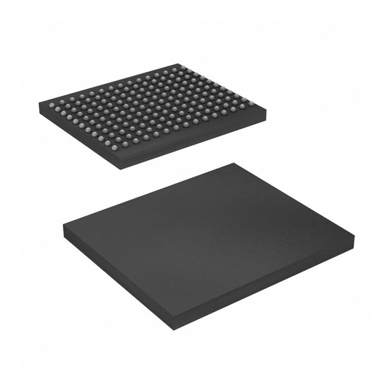
Available in 165-ball FBGA Package (13 x 15 x 1.4 mm)
■
Offered in both Pb-free and non Pb-free Packages
■
Variable Drive HSTL Output Buffers
■
JTAG 1149.1 Compatible Test Access Port
■
Phase Locked Loop (PLL) for Accurate Data Placement
■
Table 1. Selection Guide
Description
Maximum Operating Frequency
Maximum Operating Current
Cypress Semiconductor Corporation
Document Number: 001-00435 Rev. *E
= 1.4V to V
DDQ
DD
333 MHz
300 MHz
333
x8
600
x9
600
x18
620
x36
850
•
198 Champion Court
CY7C1511KV18, CY7C1526KV18
CY7C1513KV18, CY7C1515KV18
72-Mbit QDR™-II SRAM 4-Word
Configurations
CY7C1511KV18 – 8M x 8
CY7C1526KV18 – 8M x 9
CY7C1513KV18 – 4M x 18
CY7C1515KV18 – 2M x 36
Functional Description
The CY7C1511KV18, CY7C1526KV18, CY7C1513KV18, and
CY7C1515KV18 are 1.8V Synchronous Pipelined SRAMs,
equipped with QDR-II architecture. QDR-II architecture consists
of two separate ports: the read port and the write port to access
the memory array. The read port has dedicated data outputs to
support read operations and the write port has dedicated data
inputs to support write operations. QDR-II architecture has
separate data inputs and data outputs to completely eliminate
the need to "turnaround" the data bus that exists with common
IO devices. Each port can be accessed through a common
address bus. Addresses for read and write addresses are
latched on alternate rising edges of the input (K) clock. Accesses
to the QDR-II read and write ports are independent of one
another. To maximize data throughput, both read and write ports
are equipped with DDR interfaces. Each address location is
associated with four 8-bit words (CY7C1511KV18), 9-bit words
(CY7C1526KV18), 18-bit words (CY7C1513KV18), or 36-bit
words (CY7C1515KV18) that burst sequentially into or out of the
device. Because data can be transferred into and out of the
device on every rising edge of both input clocks (K and K and C
and C), memory bandwidth is maximized while simplifying
system design by eliminating bus "turnarounds".
Depth expansion is accomplished with port selects, which
enables each port to operate independently.
All synchronous inputs pass through input registers controlled by
the K or K input clocks. All data outputs pass through output
registers controlled by the C or C (or K or K in a single clock
domain) input clocks. Writes are conducted with on-chip
synchronous self-timed write circuitry.
250 MHz
200 MHz
300
250
560
490
560
490
570
500
790
680
,
•
San Jose
CA 95134-1709
Burst Architecture
167 MHz
200
167
430
380
430
380
440
390
580
510
•
408-943-2600
Revised March 30, 2009
Unit
MHz
mA
[+] Feedback
Advertisement
Table of Contents

Related Manuals for Cypress Semiconductor Perform CY7C1511KV18


Summary of Contents for Cypress Semiconductor Perform CY7C1511KV18
-
Page 1: Functional Description
Features Separate Independent Read and Write Data Ports ■ Supports concurrent transactions ❐ 333 MHz Clock for High Bandwidth ■ 4-word Burst for Reducing Address Bus Frequency ■ Double Data Rate (DDR) Interfaces on both Read and Write ■ Ports (data transferred at 666 MHz) at 333 MHz Two Input Clocks (K and K) for precise DDR Timing ■... - Page 2 Logic Block Diagram (CY7C1511KV18) [7:0] Address (20:0) Register Gen. DOFF Control Logic [1:0] Logic Block Diagram (CY7C1526KV18) [8:0] Address (20:0) Register Gen. DOFF Control Logic Document Number: 001-00435 Rev. *E CY7C1511KV18, CY7C1526KV18 CY7C1513KV18, CY7C1515KV18 Write Write Write Write Address Register Control Logic Read Data Reg.
- Page 3 Logic Block Diagram (CY7C1513KV18) [17:0] Address (19:0) Register Gen. DOFF Control Logic [1:0] Logic Block Diagram (CY7C1515KV18) [35:0] Address (18:0) Register Gen. DOFF Control Logic [3:0] Document Number: 001-00435 Rev. *E CY7C1511KV18, CY7C1526KV18 CY7C1513KV18, CY7C1515KV18 Write Write Write Write Address Register Control Logic...
-
Page 4: Pin Configuration
Pin Configuration The pin configurations for CY7C1511KV18, CY7C1526KV18, CY7C1513KV18, and CY7C1515KV18 follow. DOFF DOFF Note 1. NC/144M and NC/288M are not connected to the die and can be tied to any voltage level. Document Number: 001-00435 Rev. *E CY7C1511KV18, CY7C1526KV18 CY7C1513KV18, CY7C1515KV18 165-Ball FBGA (13 x 15 x 1.4 mm) Pinout CY7C1511KV18 (8M x 8) - Page 5 Pin Configuration (continued) The pin configurations for CY7C1511KV18, CY7C1526KV18, CY7C1513KV18, and CY7C1515KV18 follow. NC/144M DOFF NC/288M DOFF Document Number: 001-00435 Rev. *E CY7C1511KV18, CY7C1526KV18 CY7C1513KV18, CY7C1515KV18 165-Ball FBGA (13 x 15 x 1.4 mm) Pinout CY7C1513KV18 (4M x 18) NC/288M CY7C1515KV18 (2M x 36) NC/144M Page 5 of 31...
-
Page 6: Pin Definitions
Pin Definitions Pin Name Input- Data Input Signals. Sampled on the rising edge of K and K clocks when valid write operations are active. [x:0] CY7C1511KV18 − D Synchronous CY7C1526KV18 − D CY7C1513KV18 − D CY7C1515KV18 − D Write Port Select − Active LOW. Sampled on the rising edge of the K clock. When asserted active, a Input- Synchronous write operation is initiated. - Page 7 Pin Definitions (continued) Pin Name Echo Clock CQ Referenced with Respect to C. This is a free running clock and is synchronized to the input clock for output data (C) of the QDR-II. In the single clock mode, CQ is generated with respect to K. The timings for the echo clocks are shown in the Echo Clock CQ Referenced with Respect to C.
-
Page 8: Functional Overview
Functional Overview CY7C1511KV18, CY7C1526KV18, CY7C1515KV18 are synchronous pipelined Burst SRAMs with a read port and a write port. The read port is dedicated to read operations and the write port is dedicated to write operations. Data flows into the SRAM through the write port and flows out through the read port. -
Page 9: Single Clock Mode
Single Clock Mode The CY7C1511KV18 is used with a single clock that controls both the input and output registers. In this mode the device recognizes only a single pair of input clocks (K and K) that control both the input and output registers. This operation is identical to the operation if the device had zero skew between the K/K and C/C clocks. -
Page 10: Application Example
Application Example Figure 1 shows four QDR-II used in an application. DATA IN DATA OUT Address RPS# WPS# MASTER BWS# (CPU CLKIN/CLKIN# Source K ASIC) Source K# Delayed K Delayed K# R = 50ohms Truth Table The truth table for CY7C1511KV18, CY7C1526KV18, CY7C1513KV18, and CY7C1515KV18 follows. Operation RPS WPS Write Cycle:... - Page 11 Write Cycle Descriptions The write cycle description table for CY7C1511KV18 and CY7C1513KV18 follows. L–H – During the data portion of a write sequence: CY7C1511KV18 − both nibbles (D CY7C1513KV18 − both bytes (D – L-H During the data portion of a write sequence: CY7C1511KV18 −...
- Page 12 Write Cycle Descriptions The write cycle description table for CY7C1515KV18 follows. L–H – L–H – L–H – L–H – L–H – L–H – Document Number: 001-00435 Rev. *E CY7C1511KV18, CY7C1526KV18 CY7C1513KV18, CY7C1515KV18 [2, 10] Comments – During the data portion of a write sequence, all four bytes (D the device.
- Page 13 IEEE 1149.1 Serial Boundary Scan (JTAG) These SRAMs incorporate a serial boundary scan Test Access Port (TAP) in the FBGA package. This part is fully compliant with IEEE Standard #1149.1-2001. The TAP operates using JEDEC standard 1.8V IO logic levels. Disabling the JTAG Feature It is possible to operate the SRAM without using the JTAG feature.
- Page 14 IDCODE The IDCODE instruction loads a vendor-specific, 32-bit code into the instruction register. It also places the instruction register between the TDI and TDO pins and shifts the IDCODE out of the device when the TAP controller enters the Shift-DR state. The IDCODE instruction is loaded into the instruction register at power up or whenever the TAP controller is supplied a Test-Logic-Reset state.
-
Page 15: Tap Controller State Diagram
TAP Controller State Diagram The state diagram for the TAP controller follows. TEST-LOGIC RESET TEST-LOGIC/ IDLE Note 11. The 0/1 next to each state represents the value at TMS at the rising edge of TCK. Document Number: 001-00435 Rev. *E CY7C1511KV18, CY7C1526KV18 CY7C1513KV18, CY7C1515KV18 [11]... - Page 16 TAP Controller Block Diagram Selection Circuitry TAP Electrical Characteristics [12, 13, 14] Over the Operating Range Parameter Description Output HIGH Voltage Output HIGH Voltage Output LOW Voltage Output LOW Voltage Input HIGH Voltage Input LOW Voltage Input and Output Load Current Notes 12.
- Page 17 TAP AC Switching Characteristics [15, 16] Over the Operating Range Parameter TCK Clock Cycle Time TCYC TCK Clock Frequency TCK Clock HIGH TCK Clock LOW Setup Times TMS Setup to TCK Clock Rise TMSS TDI Setup to TCK Clock Rise TDIS Capture Setup to TCK Rise Hold Times...
-
Page 18: Instruction Codes
Identification Register Definitions Instruction Field CY7C1511KV18 Revision Number (31:29) Cypress Device ID 11010011011000100 11010011011001100 11010011011010100 11010011011100100 Defines the type of (28:12) Cypress JEDEC ID 00000110100 (11:1) ID Register Presence (0) Scan Register Sizes Register Name Instruction Bypass Boundary Scan Instruction Codes Instruction Code EXTEST... - Page 19 Boundary Scan Order Bit # Bump ID Bit # Document Number: 001-00435 Rev. *E CY7C1511KV18, CY7C1526KV18 CY7C1513KV18, CY7C1515KV18 Bump ID Bit # Bump ID Bit # Bump ID Internal Page 19 of 31 [+] Feedback...
-
Page 20: Power-Up Sequence
Power Up Sequence in QDR-II SRAM QDR-II SRAMs must be powered up and initialized in a predefined manner to prevent undefined operations. Power Up Sequence Apply power and drive DOFF either HIGH or LOW (All other ■ inputs can be HIGH or LOW). Apply V before V ❐... -
Page 21: Maximum Ratings
Maximum Ratings Exceeding maximum ratings may impair the useful life of the device. These user guidelines are not tested. Storage Temperature ... –65°C to +150°C Ambient Temperature with Power Applied.. –55°C to +125°C Supply Voltage on V Relative to GND ...–0.5V to +2.9V Supply Voltage on V Relative to GND...–0.5V to +V DC Applied to Outputs in High-Z ... -
Page 22: Ac Electrical Characteristics
Electrical Characteristics (continued) DC Electrical Characteristics [14] Over the Operating Range Parameter Description [21] Operating Supply Automatic Power Down Current AC Electrical Characteristics [13] Over the Operating Range Parameter Description Input HIGH Voltage Input LOW Voltage Document Number: 001-00435 Rev. *E CY7C1511KV18, CY7C1526KV18 CY7C1513KV18, CY7C1515KV18 Test Conditions... -
Page 23: Thermal Resistance
Capacitance Tested initially and after any design or process change that may affect these parameters. Parameter Description Input Capacitance Output Capacitance Thermal Resistance Tested initially and after any design or process change that may affect these parameters. Parameter Description Θ Thermal Resistance (Junction to Ambient) Θ... -
Page 24: Switching Characteristics
Switching Characteristics [22, 23] Over the Operating Range Cypress Consortium Description Parameter Parameter (Typical) to the First Access POWER K Clock and C Clock Cycle Time KHKH Input Clock (K/K; C/C) HIGH KHKL Input Clock (K/K; C/C) LOW KLKH K Clock Rise to K Clock Rise and C KHKH KHKH to C Rise (rising edge to rising edge) - Page 25 Switching Characteristics (continued) [22, 23] Over the Operating Range Cypress Consortium Description Parameter Parameter Output Times C/C Clock Rise (or K/K in single CHQV clock mode) to Data Valid Data Output Hold after Output C/C CHQX Clock Rise (Active to Active) C/C Clock Rise to Echo Clock Valid CCQO CHCQV...
-
Page 26: Switching Waveforms
Switching Waveforms Figure 5. Read/Write/Deselect Sequence READ t KH t KL t HC t SA t HA t KHCH t KHCH t CYC t CQH t CQHCQH Notes 28. Q00 refers to output from address A0. Q01 refers to output from the next internal burst address following A0, that is, A0+1. 29. -
Page 27: Ordering Information
Ordering Information The following table lists all possible speed, package, and temperature range options supported for these devices. Note that some options listed may not be available for order entry. To verify the availability of a specific option, visit the Cypress website at www.cypress.com and refer to the product summary page at representative for the status of availability of parts. - Page 28 Table 2. Ordering Information (continued) Speed (MHz) Ordering Code CY7C1511KV18-250BZC CY7C1526KV18-250BZC CY7C1513KV18-250BZC CY7C1515KV18-250BZC CY7C1511KV18-250BZXC CY7C1526KV18-250BZXC CY7C1513KV18-250BZXC CY7C1515KV18-250BZXC CY7C1511KV18-250BZI CY7C1526KV18-250BZI CY7C1513KV18-250BZI CY7C1515KV18-250BZI CY7C1511KV18-250BZXI CY7C1526KV18-250BZXI CY7C1513KV18-250BZXI CY7C1515KV18-250BZXI CY7C1511KV18-200BZC CY7C1526KV18-200BZC CY7C1513KV18-200BZC CY7C1515KV18-200BZC CY7C1511KV18-200BZXC CY7C1526KV18-200BZXC CY7C1513KV18-200BZXC CY7C1515KV18-200BZXC CY7C1511KV18-200BZI CY7C1526KV18-200BZI CY7C1513KV18-200BZI CY7C1515KV18-200BZI CY7C1511KV18-200BZXI CY7C1526KV18-200BZXI CY7C1513KV18-200BZXI CY7C1515KV18-200BZXI Document Number: 001-00435 Rev.
- Page 29 Table 2. Ordering Information (continued) Speed (MHz) Ordering Code CY7C1511KV18-167BZC CY7C1526KV18-167BZC CY7C1513KV18-167BZC CY7C1515KV18-167BZC CY7C1511KV18-167BZXC CY7C1526KV18-167BZXC CY7C1513KV18-167BZXC CY7C1515KV18-167BZXC CY7C1511KV18-167BZI CY7C1526KV18-167BZI CY7C1513KV18-167BZI CY7C1515KV18-167BZI CY7C1511KV18-167BZXI CY7C1526KV18-167BZXI CY7C1513KV18-167BZXI CY7C1515KV18-167BZXI Document Number: 001-00435 Rev. *E CY7C1511KV18, CY7C1526KV18 CY7C1513KV18, CY7C1515KV18 Package Diagram Package Type 51-85180 165-Ball Fine Pitch Ball Grid Array (13 x 15 x 1.4 mm) 51-85180 165-Ball Fine Pitch Ball Grid Array (13 x 15 x 1.4 mm) Pb-Free 51-85180 165-Ball Fine Pitch Ball Grid Array (13 x 15 x 1.4 mm) 51-85180 165-Ball Fine Pitch Ball Grid Array (13 x 15 x 1.4 mm) Pb-Free...
-
Page 30: Package Diagram
Package Diagram Figure 6. 165-Ball FBGA (13 x 15 x 1.4 mm), 51-85180 TOP VIEW PIN 1 CORNER 13.00±0.10 SEATING PLANE Document Number: 001-00435 Rev. *E CY7C1511KV18, CY7C1526KV18 CY7C1513KV18, CY7C1515KV18 0.15(4X) BOTTOM VIEW PIN 1 CORNER Ø0.05 M C Ø0.25 M C A B -0.06 Ø0.50 (165X) +0.14... - Page 31 Document History Page Document Title: CY7C1511KV18/CY7C1526KV18/CY7C1513KV18/CY7C1515KV18, 72-Mbit QDR™-II SRAM 4-Word Burst Architecture Document Number: 001-00435 Orig. of Submission Rev. ECN No. Change Date 374703 See ECN 1103823 See ECN 1699083 VKN/AESA See ECN 2148307 VKN/AESA See ECN 2606839 VKN/PYRS 11/13/08 2681899 VKN/PYRS 04/01/2009 Sales, Solutions, and Legal Information...
Need help?
Do you have a question about the Perform CY7C1511KV18 and is the answer not in the manual?
Questions and answers