Table of Contents
Advertisement
Quick Links
Features
Separate Independent Read and Write Data Ports
■
Supports concurrent transactions
❐
333 MHz Clock for High Bandwidth
■
2-word Burst on all Accesses
■
Double Data Rate (DDR) Interfaces on both Read and Write
■
Ports (data transferred at 666 MHz) at 333 MHz
Two Input Clocks (K and K) for precise DDR timing
■
SRAM uses rising edges only
❐
Two Input Clocks for Output Data (C and C) to minimize Clock
■
Skew and Flight Time mismatches
Echo Clocks (CQ and CQ) simplify Data Capture in High Speed
■
Systems
Single Multiplexed Address Input bus latches Address Inputs
■
for both Read and Write Ports
Separate Port Selects for Depth Expansion
■
Synchronous internally Self-timed Writes
■
QDR™-II operates with 1.5 Cycle Read Latency when DOFF
■
is asserted HIGH
Operates similar to QDR-I Device with 1 Cycle Read Latency
■
when DOFF is asserted LOW
Available in x8, x9, x18, and x36 Configurations
■
Full Data Coherency, providing Most Current Data
■
Core V
= 1.8V (±0.1V); IO V
■
DD
Supports both 1.5V and 1.8V IO supply
❐
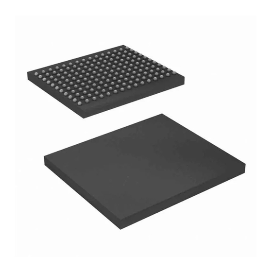
Available in 165-ball FBGA Package (13 x 15 x 1.4 mm)
■
Offered in both Pb-free and non Pb-free Packages
■
Variable Drive HSTL Output Buffers
■
JTAG 1149.1 Compatible Test Access Port
■
Phase Locked Loop (PLL) for Accurate Data Placement
■
Table 1. Selection Guide
Description
Maximum Operating Frequency
Maximum Operating Current
Cypress Semiconductor Corporation
Document Number: 001-00436 Rev. *E
= 1.4V to V
DDQ
DD
333 MHz
300 MHz
333
x8
790
x9
790
x18
810
x36
990
•
198 Champion Court
CY7C1510KV18, CY7C1525KV18
CY7C1512KV18, CY7C1514KV18
72-Mbit QDR™-II SRAM 2-Word
Configurations
CY7C1510KV18 – 8M x 8
CY7C1525KV18 – 8M x 9
CY7C1512KV18 – 4M x 18
CY7C1514KV18 – 2M x 36
Functional Description
The CY7C1510KV18, CY7C1525KV18, CY7C1512KV18, and
CY7C1514KV18 are 1.8V Synchronous Pipelined SRAMs,
equipped with QDR-II architecture. QDR-II architecture consists
of two separate ports: the read port and the write port to access
the memory array. The read port has dedicated data outputs to
support read operations and the write port has dedicated data
inputs to support write operations. QDR-II architecture has
separate data inputs and data outputs to completely eliminate
the need to "turnaround" the data bus that exists with common
I/O devices. Access to each port is through a common address
bus. Addresses for read and write addresses are latched on
alternate rising edges of the input (K) clock. Accesses to the
QDR-II read and write ports are completely independent of one
another. To maximize data throughput, both read and write ports
are equipped with DDR interfaces. Each address location is
associated with two 8-bit words (CY7C1510KV18), 9-bit words
(CY7C1525KV18), 18-bit words (CY7C1512KV18), or 36-bit
words (CY7C1514KV18) that burst sequentially into or out of the
device. Because data can be transferred into and out of the
device on every rising edge of both input clocks (K and K and C
and C), memory bandwidth is maximized while simplifying
system design by eliminating bus turnarounds.
Depth expansion is accomplished with port selects, which
enables each port to operate independently.
All synchronous inputs pass through input registers controlled by
the K or K input clocks. All data outputs pass through output
registers controlled by the C or C (or K or K in a single clock
domain) input clocks. Writes are conducted with on-chip
synchronous self-timed write circuitry.
250 MHz
200 MHz
300
250
730
640
730
640
750
650
910
790
,
•
San Jose
CA 95134-1709
Burst Architecture
167 MHz
200
167
MHz
540
480
540
480
550
490
660
580
•
408-943-2600
Revised March 30, 2009
Unit
mA
[+] Feedback
Advertisement
Table of Contents

Related Manuals for Cypress Semiconductor CY7C1510KV18


Summary of Contents for Cypress Semiconductor CY7C1510KV18
-
Page 1: Functional Description
To maximize data throughput, both read and write ports are equipped with DDR interfaces. Each address location is associated with two 8-bit words (CY7C1510KV18), 9-bit words (CY7C1525KV18), 18-bit words (CY7C1512KV18), or 36-bit words (CY7C1514KV18) that burst sequentially into or out of the device. - Page 2 Logic Block Diagram (CY7C1510KV18) [7:0] Address (21:0) Register Gen. DOFF Control Logic [1:0] Logic Block Diagram (CY7C1525KV18) [8:0] Address (21:0) Register Gen. DOFF Control Logic Document Number: 001-00436 Rev. *E CY7C1510KV18, CY7C1525KV18 CY7C1512KV18, CY7C1514KV18 Write Write Address Register Control Logic Read Data Reg.
- Page 3 Control Logic [1:0] Logic Block Diagram (CY7C1514KV18) [35:0] Address (19:0) Register Gen. DOFF Control Logic [3:0] Document Number: 001-00436 Rev. *E CY7C1510KV18, CY7C1525KV18 CY7C1512KV18, CY7C1514KV18 Write Write Address Register Control Logic Read Data Reg. Reg. Reg. Reg. Write Write Address...
-
Page 4: Pin Configuration
Pin Configuration The pin configurations for CY7C1510KV18, CY7C1525KV18, CY7C1512KV18, and CY7C1514KV18 follow. DOFF DOFF Note 1. NC/144M and NC/288M are not connected to the die and can be tied to any voltage level. Document Number: 001-00436 Rev. *E CY7C1510KV18, CY7C1525KV18 CY7C1512KV18, CY7C1514KV18 165-Ball FBGA (13 x 15 x 1.4 mm) Pinout... - Page 5 Pin Configuration (continued) The pin configurations for CY7C1510KV18, CY7C1525KV18, CY7C1512KV18, and CY7C1514KV18 follow. NC/144M DOFF NC/288M DOFF Document Number: 001-00436 Rev. *E CY7C1510KV18, CY7C1525KV18 CY7C1512KV18, CY7C1514KV18 165-Ball FBGA (13 x 15 x 1.4 mm) Pinout CY7C1512KV18 (4M x 18) NC/288M...
-
Page 6: Pin Definitions
These address inputs are multiplexed for both read and write operations. Internally, the device is organized as 8M x 8 (2 arrays each of 4M x 8) for CY7C1510KV18, 8M x 9 (2 arrays each of 4M x 9) for CY7C1525KV18, 4M x 18 (2 arrays each of 2M x 18) for CY7C1512KV18, and 2M x 36 (2 arrays each of 1M x 36) for CY7C1514KV18. - Page 7 Power Supply Power Supply Inputs to the Core of the Device. Ground Ground for the device. Power Supply Power Supply Inputs for the Outputs of the Device. Document Number: 001-00436 Rev. *E CY7C1510KV18, CY7C1525KV18 CY7C1512KV18, CY7C1514KV18 Pin Description Switching Characteristics on page 23.
-
Page 8: Functional Overview
Single Clock Mode The CY7C1510KV18 is used with a single clock that controls both the input and output registers. In this mode the device recognizes only a single pair of input clocks (K and K) that control both the input and output registers. -
Page 9: Application Example
Delayed K Delayed K# R = 50ohms Document Number: 001-00436 Rev. *E CY7C1510KV18, CY7C1525KV18 CY7C1512KV18, CY7C1514KV18 These chips use a PLL that is designed to function between 120 MHz and the specified maximum clock frequency. During power up, when the DOFF is tied HIGH, the PLL is locked after 20 μs of stable clock. -
Page 10: Truth Table
Truth Table The truth table for CY7C1510KV18, CY7C1525KV18, CY7C1512KV18, and CY7C1514KV18 follow. Operation Write Cycle: Load address on the rising edge of K; input write data on K and K rising edges. Read Cycle: Load address on the rising edge of K;... - Page 11 – L–H – L–H – L–H – Document Number: 001-00436 Rev. *E CY7C1510KV18, CY7C1525KV18 CY7C1512KV18, CY7C1514KV18 [2, 8] [2, 8] Comments – During the data portion of a write sequence, all four bytes (D the device. L–H During the data portion of a write sequence, all four bytes (D the device.
- Page 12 TDI pin on the rising edge of TCK. Data is output on the TDO pin on the falling edge of TCK. Document Number: 001-00436 Rev. *E CY7C1510KV18, CY7C1525KV18 CY7C1512KV18, CY7C1514KV18 Instruction Register Three-bit instructions are serially loaded into the instruction register.
- Page 13 Document Number: 001-00436 Rev. *E CY7C1510KV18, CY7C1525KV18 CY7C1512KV18, CY7C1514KV18 BYPASS When the BYPASS instruction is loaded in the instruction register and the TAP is placed in a Shift-DR state, the bypass register is placed between the TDI and TDO pins.
-
Page 14: Tap Controller State Diagram
The state diagram for the TAP controller follows. TEST-LOGIC RESET TEST-LOGIC/ IDLE Note 9. The 0/1 next to each state represents the value at TMS at the rising edge of TCK. Document Number: 001-00436 Rev. *E CY7C1510KV18, CY7C1525KV18 CY7C1512KV18, CY7C1514KV18 SELECT DR-SCAN CAPTURE-DR SHIFT-DR EXIT1-DR PAUSE-DR... - Page 15 10. These characteristics pertain to the TAP inputs (TMS, TCK, TDI and TDO). Parallel load levels are specified in the 11. Overshoot: V (AC) < V + 0.85V (Pulse width less than t 12. All voltage referenced to Ground. Document Number: 001-00436 Rev. *E CY7C1510KV18, CY7C1525KV18 CY7C1512KV18, CY7C1514KV18 Bypass Register Instruction Register Identification Register Boundary Scan Register...
- Page 16 14. Test conditions are specified using the load in TAP AC Test Conditions. t Document Number: 001-00436 Rev. *E CY7C1510KV18, CY7C1525KV18 CY7C1512KV18, CY7C1514KV18 Description [14] Figure 2.
-
Page 17: Instruction Codes
RESERVED Do Not Use: This instruction is reserved for future use. BYPASS Places the bypass register between TDI and TDO. This operation does not affect SRAM operation. Document Number: 001-00436 Rev. *E CY7C1510KV18, CY7C1525KV18 CY7C1512KV18, CY7C1514KV18 Value CY7C1525KV18 CY7C1512KV18 11010011010001100... - Page 18 Boundary Scan Order Bit # Bump ID Bit # Document Number: 001-00436 Rev. *E CY7C1510KV18, CY7C1525KV18 CY7C1512KV18, CY7C1514KV18 Bump ID Bit # Bump ID Bit # Bump ID Internal Page 18 of 30 [+] Feedback...
- Page 19 PLL. Unstable Clock Clock Start (Clock Starts after DOFF Document Number: 001-00436 Rev. *E CY7C1510KV18, CY7C1525KV18 CY7C1512KV18, CY7C1514KV18 PLL Constraints PLL uses K clock as its synchronizing input. The input must ■ have low phase jitter, which is specified as t The PLL functions at frequencies down to 120 MHz.
-
Page 20: Maximum Ratings
, whichever is larger, V 19. The operation current is calculated with 50% read cycle and 50% write cycle. Document Number: 001-00436 Rev. *E CY7C1510KV18, CY7C1525KV18 CY7C1512KV18, CY7C1514KV18 Current into Outputs (LOW) ... 20 mA Static Discharge Voltage (MIL-STD-883, M. 3015).. > 2001V Latch up Current... -
Page 21: Ac Electrical Characteristics
AC Electrical Characteristics [11] Over the Operating Range Parameter Description Input HIGH Voltage Input LOW Voltage Document Number: 001-00436 Rev. *E CY7C1510KV18, CY7C1525KV18 CY7C1512KV18, CY7C1514KV18 Test Conditions = Max, 200 MHz (x8) = 0 mA, (x9) f = f = 1/t... -
Page 22: Thermal Resistance
20. Unless otherwise noted, test conditions are based on signal transition time of 2V/ns, timing reference levels of 0.75V, Vref = 0.75V, RQ = 250Ω, V pulse levels of 0.25V to 1.25V, and output loading of the specified I Document Number: 001-00436 Rev. *E CY7C1510KV18, CY7C1525KV18 CY7C1512KV18, CY7C1514KV18 Test Conditions = 25°C, f = 1 MHz, V... -
Page 23: Switching Characteristics
22. This part has a voltage regulator internally; t POWER Document Number: 001-00436 Rev. *E CY7C1510KV18, CY7C1525KV18 CY7C1512KV18, CY7C1514KV18 333 MHz 300 MHz Min Max Min Max Min Max Min Max Min Max [22] 1.20... - Page 24 , are specified with a load capacitance of 5 pF as in part (b) of 25. At any voltage and temperature t is less than t Document Number: 001-00436 Rev. *E CY7C1510KV18, CY7C1525KV18 CY7C1512KV18, CY7C1514KV18 333 MHz 300 MHz Min Max Min Max Min Max Min Max Min Max –...
-
Page 25: Switching Waveforms
28. In this example, if address A0 = A1, then data Q00 = D10 and Q01 = D11. Write data is forwarded immediately as read results. This note applies to the whole diagram. Document Number: 001-00436 Rev. *E CY7C1510KV18, CY7C1525KV18 CY7C1512KV18, CY7C1514KV18... -
Page 26: Ordering Information
CY7C1512KV18-300BZI CY7C1514KV18-300BZI CY7C1510KV18-300BZXI CY7C1525KV18-300BZXI CY7C1512KV18-300BZXI CY7C1514KV18-300BZXI Document Number: 001-00436 Rev. *E CY7C1510KV18, CY7C1525KV18 CY7C1512KV18, CY7C1514KV18 http://www.cypress.com/products Package Diagram Package Type 51-85180 165-Ball Fine Pitch Ball Grid Array (13 x 15 x 1.4 mm) 51-85180 165-Ball Fine Pitch Ball Grid Array (13 x 15 x 1.4 mm) Pb-Free 51-85180 165-Ball Fine Pitch Ball Grid Array (13 x 15 x 1.4 mm) - Page 27 CY7C1514KV18-200BZI CY7C1510KV18-200BZXI CY7C1525KV18-200BZXI CY7C1512KV18-200BZXI CY7C1514KV18-200BZXI Document Number: 001-00436 Rev. *E CY7C1510KV18, CY7C1525KV18 CY7C1512KV18, CY7C1514KV18 Package Diagram Package Type 51-85180 165-Ball Fine Pitch Ball Grid Array (13 x 15 x 1.4 mm) 51-85180 165-Ball Fine Pitch Ball Grid Array (13 x 15 x 1.4 mm) Pb-Free 51-85180 165-Ball Fine Pitch Ball Grid Array (13 x 15 x 1.4 mm)
- Page 28 CY7C1514KV18-167BZI CY7C1510KV18-167BZXI CY7C1525KV18-167BZXI CY7C1512KV18-167BZXI CY7C1514KV18-167BZXI Document Number: 001-00436 Rev. *E CY7C1510KV18, CY7C1525KV18 CY7C1512KV18, CY7C1514KV18 Package Diagram Package Type 51-85180 165-Ball Fine Pitch Ball Grid Array (13 x 15 x 1.4 mm) 51-85180 165-Ball Fine Pitch Ball Grid Array (13 x 15 x 1.4 mm) Pb-Free 51-85180 165-Ball Fine Pitch Ball Grid Array (13 x 15 x 1.4 mm)
-
Page 29: Package Diagram
Figure 6. 165-Ball FBGA (13 x 15 x 1.4 mm), 51-85180 TOP VIEW PIN 1 CORNER 13.00±0.10 SEATING PLANE Document Number: 001-00436 Rev. *E CY7C1510KV18, CY7C1525KV18 CY7C1512KV18, CY7C1514KV18 0.15(4X) BOTTOM VIEW PIN 1 CORNER Ø0.05 M C Ø0.25 M C A B -0.06... - Page 30 Document History Page Document Title: CY7C1510KV18/CY7C1525KV18/CY7C1512KV18/CY7C1514KV18, 72-Mbit QDR™-II SRAM 2-Word Burst Architecture Document Number: 001-00436 Orig. of Submission Rev. ECN No. Change Date 374703 See ECN 1103823 See ECN 1699083 VKN/AESA See ECN 2148307 VKN/AESA See ECN 2606839 VKN/PYRS 11/13/08...
Need help?
Do you have a question about the CY7C1510KV18 and is the answer not in the manual?
Questions and answers