Table of Contents
Advertisement
Quick Links
Features
• Very high speed: 45 ns
• Wide voltage range: 2.20V–3.60V
• Pin compatible with CY62138CV25/30/33
• Ultra low standby power
— Typical standby current: 1 µA
— Maximum standby current: 5 µA
• Ultra low active power
— Typical active current: 1.6 mA @ f = 1 MHz
• Easy memory expansion with CE
• Automatic power down when deselected
• CMOS for optimum speed and power
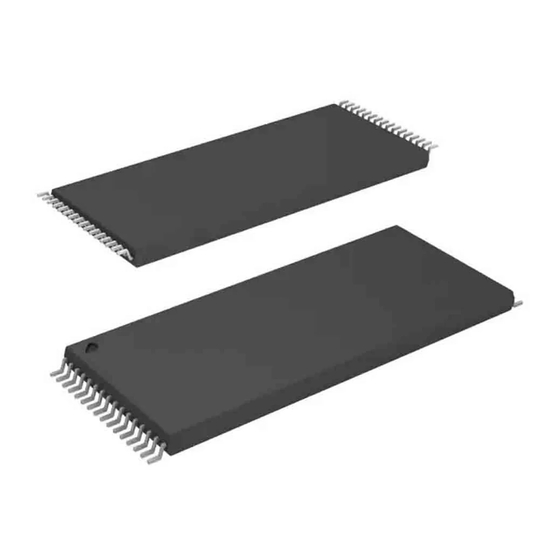
• Offered in Pb-free 36-ball VFBGA, 32-pin TSOP II, 32-pin
SOIC, 32-pin TSOP I and 32-pin STSOP packages
Logic Block Diagram
CE 1
CE 2
Note
1. For best practice recommendations, refer to the Cypress application note "System Design Guidelines" at
Cypress Semiconductor Corporation
Document #: 001-08029 Rev. *E
, CE
and OE features
1
2,
DATA IN DRIVERS
A 0
A 1
A 2
A 3
A 4
A 5
256K x 8
A 6
A 7
ARRAY
A 8
A 9
A 10
A 11
COLUMN DECODER
WE
OE
•
198 Champion Court
CY62138FV30 MoBL
2-Mbit (256K x 8) Static RAM
Functional Description
The CY62138FV30 is a high performance CMOS static RAM
organized as 256K words by 8 bits. This device features
advanced circuit design to provide ultra low active current.
This is ideal for providing More Battery Life™ (MoBL
portable applications such as cellular telephones. The device
also has an automatic power down feature that significantly
reduces power consumption. Place the device into standby
mode reducing power consumption when deselected (CE
HIGH or CE
LOW).
2
To write to the device, take Chip Enable (CE
HIGH) and Write Enable (WE) inputs LOW. Data on the eight
IO pins (IO
through IO
) is then written into the location
0
7
specified on the address pins (A
To read from the device, take Chip Enable (CE
HIGH) and Output Enable (OE) LOW while forcing Write
Enable (WE) HIGH. Under these conditions, the contents of
the memory location specified by the address pins appear on
the IO pins.
The eight input and output pins (IO
in a high impedance state when the device is deselected (CE
HIGH or CE
LOW), the outputs are disabled (OE HIGH), or
2
during a write operation (CE
LOW).
POWER
DOWN
http://www.cypress.com.
,
•
San Jose
CA 95134-1709
[1]
®
) in
LOW and CE
1
through A
).
0
17
LOW and CE
1
through IO
) are placed
0
7
LOW and CE
HIGH and WE
1
2
IO 0
IO 1
IO 2
IO 3
IO 4
IO 5
IO 6
IO 7
•
408-943-2600
Revised March 26, 2007
®
1
2
2
1
[+] Feedback
Advertisement
Table of Contents

Related Manuals for Cypress Semiconductor CY62138FV30


Summary of Contents for Cypress Semiconductor CY62138FV30
-
Page 1: Functional Description
Document #: 001-08029 Rev. *E 2-Mbit (256K x 8) Static RAM Functional Description The CY62138FV30 is a high performance CMOS static RAM organized as 256K words by 8 bits. This device features advanced circuit design to provide ultra low active current. -
Page 2: Pin Configuration
3. Typical values are included for reference only and are not guaranteed or tested. Typical values are measured at V Document #: 001-08029 Rev. *E 32-Pin SOIC/TSOP II Operating I Speed (ns) f = 1 MHz ® CY62138FV30 MoBL Top View STSOP Top View (not to scale) Power Dissipation (mA) Standby I (µA) -
Page 3: Maximum Ratings
= 3.60V Test Conditions = 25°C, f = 1 MHz, CC(typ.) (min) and 200 µs wait time after V spec. Other inputs can be left floating. CCDR ® CY62138FV30 MoBL ...–0.3V to 3.9V Ambient Range Temperature 45 ns Unit + 0.3V + 0.3V... - Page 4 DATA RETENTION MODE > 1.5V CC(min) > 100 µs or stable at V to V CC(min) CC(min) is LOW and CE is HIGH, CE is LOW; when CE CY62138FV30 MoBL TSOP II STSOP TSOP I Unit °C/W 44.16 59.72 50.19 °C/W...
-
Page 5: Switching Characteristics
HZCE LZCE HZOE LZOE , and CE . All signals must be ACTIVE to initiate a write and any of these ® CY62138FV30 MoBL 45 ns Unit /2, input CC(typ) 4” . is less than t for any given device. -
Page 6: Switching Waveforms
20. During this period, the IOs are in output state. Do not apply input signals. Document #: 001-08029 Rev. *E [15, 16] DATA VALID DATA VALID , CE transition HIGH. ® CY62138FV30 MoBL DATA VALID HZOE HZCE HIGH IMPEDANCE Page 6 of 13 [+] Feedback... -
Page 7: Truth Table
DATA VALID Inputs/Outputs High-Z Deselect/Power Down High-Z Deselect/Power Down Data Out Read High-Z Output Disabled Data in Write ® CY62138FV30 MoBL LZWE Mode Power Standby (I Standby (I Active (I Active (I Active (I Page 7 of 13 [+] Feedback... -
Page 8: Ordering Information
Figure 1. 36-ball VFBGA (6 x 8 x 1 mm), 51-85149 TOP VIEW A1 CORNER 6.00±0.10 SEATING PLANE Document #: 001-08029 Rev. *E CY62138FV30 MoBL Package Type 36-ball VFBGA (Pb-free) 32-pin TSOP II (Pb-free) 32-pin STSOP (Pb-free) 32-pin TSOP I (Pb-free) 32-pin SOIC (Pb-free) 0.15(4X) - Page 9 ® CY62138FV30 MoBL Package Diagrams (continued) Figure 2. 32-pin TSOP II, 51-85095 51-85095-** Document #: 001-08029 Rev. *E Page 9 of 13 [+] Feedback...
- Page 10 0.793[20.142] 0.817[20.751] 0.101[2.565] 0.111[2.819] 0.050[1.270] BSC. 0.014[0.355] 0.020[0.508] Document #: 001-08029 Rev. *E 0.546[13.868] 0.566[14.376] 0.440[11.176] 0.450[11.430] 0.006[0.152] 0.012[0.304] 0.118[2.997] MAX. 0.004[0.102] 0.004[0.102] MIN. SEATING PLANE ® CY62138FV30 MoBL 0.047[1.193] 0.063[1.600] 0.023[0.584] 0.039[0.990] 51-85081-*B Page 10 of 13 [+] Feedback...
- Page 11 ® CY62138FV30 MoBL Package Diagrams (continued) Figure 4. 32-pin TSOP I (8 x 20 mm), 51-85056 51-85056-*D Document #: 001-08029 Rev. *E Page 11 of 13 [+] Feedback...
- Page 12 ® CY62138FV30 MoBL Package Diagrams (continued) Figure 5. 32-pin STSOP (8 x 13.4 mm), 51-85094 51-85094-*D MoBL is a registered trademark, and More Battery Life is a trademark of Cypress Semiconductor. All product and company names mentioned in this document may be the trademarks of their respective holders.
- Page 13 Document History Page Document Title: CY62138FV30 MoBL Document Number: 001-08029 Issue Orig. of REV. ECN NO. Date Change 463660 See ECN 467351 See ECN 566724 See ECN 797956 See ECN 809101 See ECN 940341 See ECN Document #: 001-08029 Rev. *E ®...
Need help?
Do you have a question about the CY62138FV30 and is the answer not in the manual?
Questions and answers