Table of Contents
Advertisement
Quick Links
Features
• High speed
— 10 ns
• Fast t
DOE
• CMOS for optimum speed/power
• Low active power
— 467 mW (max, 12 ns "L" version)
• Low standby power
— 0.275 mW (max, "L" version)
• 2V data retention ("L" version only)
• Easy memory expansion with CE and OE features
• TTL-compatible inputs and outputs
• Automatic power-down when deselected
Functional Description
The CY7C199 is a high-performance CMOS static RAM orga-
nized as 32,768 words by 8 bits. Easy memory expansion is
Logic Block Diagram
INPUT BUFFER
A
0
A
1
A
2
A
3
A
4
A
1024 x 32 x 8
5
ARRAY
A
6
A
7
A
8
A
9
CE
WE
COLUMN
DECODER
OE
Selection Guide
Maximum Access Time (ns)
Maximum Operating
Current (mA)
L
Maximum CMOS
Standby Current (mA)
L
Shaded area contains advance information.
Cypress Semiconductor Corporation
Document #: 38-05160 Rev. **
POWER
DOWN
C199–1
7C199-8
7C199-10 7C199-12 7C199-15 7C199-20 7C199-25 7C199-35 7C199-45
8
10
120
110
160
90
0.5
0.5
0.05
0.05
•
3901 North First Street
provided by an active LOW Chip Enable (CE) and active LOW
Output Enable (OE) and three-state drivers. This device has
an automatic power-down feature, reducing the power con-
sumption by 81% when deselected. The CY7C199 is in the
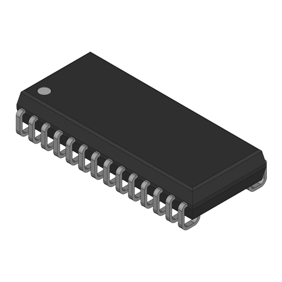
standard 300-mil-wide DIP, SOJ, and LCC packages.
An active LOW Write Enable signal (WE) controls the writ-
ing/reading operation of the memory. When CE and WE inputs
are both LOW, data on the eight data input/output pins (I/O
through I/O
) is written into the memory location addressed by
7
the address present on the address pins (A
Reading the device is accomplished by selecting the device
and enabling the outputs, CE and OE active LOW, while WE
remains inactive or HIGH. Under these conditions, the con-
tents of the location addressed by the information on address
pins are present on the eight data input/output pins.
The input/output pins remain in a high-impedance state unless
the chip is selected, outputs are enabled, and Write Enable
(WE) is HIGH. A die coat is used to improve alpha immunity.
Pin Configurations
DIP / SOJ / SOIC
Top View
A
28
1
5
A
2
27
6
A
26
3
7
A
8
4
25
24
A
5
9
A
23
6
10
A
22
11
7
I/O
A
21
0
12
8
A
20
9
13
A
19
10
I/O
14
1
18
I/O
11
0
17
12
I/O
1
I/O
2
16
I/O
13
2
15
GND
14
I/O
3
OE
22
A
23
I/O
1
4
A
24
2
A
25
3
I/O
5
A
26
4
WE
27
28
I/O
V
CC
6
A
1
5
A
2
6
I/O
A
3
7
7
A
4
8
A
5
9
A
6
10
A
7
11
12
15
20
155
150
90
90
90
10
10
10
0.05
0.05
•
San Jose
CY7C199
32K x 8 Static RAM
through A
0
LCC
Top View
V
CC
WE
3 2 1
28
27
A
4
4
26
A
8
A
3
5
25
A
9
A
A
6
24
2
10
A
A
7
23
1
11
A
8
22
12
OE
A
9
21
13
A
0
A
10
20
14
CE
11
19
I/O
0
I/O
7
12
18
I/O
1
I/O
6
1314151617
I/O
5
I/O
4
I/O
3
C199–2
TSOP I
Top View
(not to scale)
25
35
150
140
80
70
10
10
0.05
0.05
•
CA 95134
•
408-943-2600
Revised September 7, 2001
0
).
14
A
4
A
3
A
2
A
1
OE
A
0
CE
I/O
7
I/O
6
C199–3
A
21
0
20
CE
I/O
19
7
I/O
18
6
I/O
17
5
I/O
16
4
I/O
15
3
GND
14
I/O
13
2
I/O
12
1
I/O
11
0
A
10
14
A
9
13
8
A
12
C199–4
45
140
10
Advertisement
Table of Contents

Related Manuals for Cypress Semiconductor CY7C199


Summary of Contents for Cypress Semiconductor CY7C199
-
Page 1: Functional Description
Output Enable (OE) and three-state drivers. This device has an automatic power-down feature, reducing the power con- sumption by 81% when deselected. The CY7C199 is in the standard 300-mil-wide DIP, SOJ, and LCC packages. An active LOW Write Enable signal (WE) controls the writ- ing/reading operation of the memory. -
Page 2: Maximum Ratings
= Max., Com’l = 0 mA, = 1/t Com’l , f = f Com’l – 0.3V 0.05 – 0.3V < 0.3V, f = 0 CY7C199 ... –0.5V to V ... –0.5V to V 7C199-10 7C199-12 7C199-15 Min. Max. Min. Max. Min. - Page 3 = 25 C, f = 1 MHz, = 5.0V 7C199-25 7C199-35 7C199-45 Min. Max. Min. Max. Min. +0.3V +0.3V -0.5 -0.5 -0.5 –5 –5 –5 –5 –5 –5 0.05 0.05 Max. CY7C199 Max. Unit +0.3V 0.05 Unit Page 3 of 16...
- Page 4 Over the Operating Range (L version only) Conditions Com’l = 2.0V, CE > V – 0.3V, Com’l L > V – 0.3V or < 0.3V DATA RETENTION MODE 3.0V > 2V CY7C199 ALL INPUT PULSES 3.0V Min. Max. 3.0V C199–6 Unit C199–7 Page 4 of 16...
-
Page 5: Switching Characteristics
= 5 pF as in part (b) of AC Test Loads. Transition is measured 500 mV from steady-state voltage. HZWE 7C199-12 7C199-15 Max. Min. Max. Min. , and t is less than t for any given device. HZWE LZWE and t CY7C199 Max. Unit Page 5 of 16... -
Page 6: Write Cycle
12. Device is continuously selected. OE, CE = V 13. WE is HIGH for read cycle. Document #: 38-05160 Rev. ** [3,7] (continued) 7C199-20 7C199-25 Min. Max. Min. [8, 9] [8, 9] CY7C199 7C199-35 7C199-45 Max. Min. Max. Min. Max. DATA VALID Unit C199–8 Page 6 of 16... - Page 7 16. If CE goes HIGH simultaneously with WE HIGH, the output remains in a high-impedance state. Document #: 38-05160 Rev. ** LZOE DATA DATA HZOE HZCE DATA VALID VALID VALID CY7C199 HIGH IMPEDANCE C199–9 C199–10 C199–11 Page 7 of 16...
- Page 8 AMBIENT TEMPERATURE =5.0V –55 AMBIENT TEMPERATURE ( C) VALID LZWE OUTPUT SOURCE CURRENT vs. OUTPUT VOLTAGE OUTPUT VOLTAGE (V) OUTPUT SINK CURRENT vs. OUTPUT VOLTAGE OUTPUT VOLTAGE (V) CY7C199 C199–12 =5.0V =25 C =5.0V =25 C Page 8 of 16...
-
Page 9: Truth Table
TYPICAL POWER-ON CURRENT vs. SUPPLY VOLTAGE SUPPLY VOLTAGE (V) Truth Table Inputs/Outputs High Z Data Out Data In High Z Ordering Information Speed (ns) Ordering Code CY7C199-8VC CY7C199-8ZC CY7C199L-8VC CY7C199L-8ZC CY7C199-10VC CY7C199-10ZC CY7C199L-10VC CY7C199L-10ZC CY7C199-10VI CY7C199-10ZI CY7C199L-10VI CY7C199L-10ZI CY7C199-12PC CY7C199-12VC... - Page 10 Ordering Information (continued) Speed (ns) Ordering Code CY7C199-15PC CY7C199-15VC CY7C199-15ZC CY7C199L-15PC CY7C199L-15VC CY7C199L-15ZC CY7C199-15VI CY7C199-15ZI CY7C199-15DMB CY7C199-15LMB CY7C199L-15DMB CY7C199L-15LMB CY7C199-20PC CY7C199-20VC CY7C199-20ZC CY7C199L-20PC CY7C199L-20VC CY7C199L-20ZC CY7C199-20VI CY7C199-20ZI CY7C199-20DMB CY7C199-20LMB CY7C199L-20DMB CY7C199L-20LMB CY7C199-25PC CY7C199-25SC CY7C199-25VC CY7C199-25ZC CY7C199L-25ZI CY7C199-25DMB CY7C199-25LMB CY7C199-35PC CY7C199-35SC...
-
Page 11: Military Specifications
7, 8, 9, 10, 11 7, 8, 9, 10, 11 7, 8, 9, 10, 11 7, 8, 9, 10, 11 7, 8, 9, 10, 11 7, 8, 9, 10, 11 7, 8, 9, 10, 11 CY7C199 Page 11 of 16... -
Page 12: Package Diagrams
CY7C199 Package Diagrams 28-Lead (300-Mil) CerDIP D22 MIL-STD-1835 D-15 Config. A 51-80032 Document #: 38-05160 Rev. ** Page 12 of 16... - Page 13 CY7C199 Package Diagrams (continued) 28-Pin Rectangular Leadless Chip Carrier L54 MIL-STD-1835 C-11A 51-80067 28-Lead (300-Mil) Molded DIP P21 51-85014-B Document #: 38-05160 Rev. ** Page 13 of 16...
- Page 14 Package Diagrams (continued) Document #: 38-05160 Rev. ** 28-Lead (300-Mil) Molded SOIC S21 28-Lead (300-Mil) Molded SOJ V21 CY7C199 51-85026-A 51-85031-B Page 14 of 16...
- Page 15 CY7C199 Package Diagrams (continued) 28-Lead Thin Small Outline Package Z28 51-85071-F Document #: 38-05160 Rev. ** Page 15 of 16 © Cypress Semiconductor Corporation, 2001. The information contained herein is subject to change without notice. Cypress Semiconductor Corporation assumes no responsibility for the use of any circuitry other than circuitry embodied in a Cypress Semiconductor product.
- Page 16 Document Title: CY7C199 32K x 8 Static RAM Document Number: 38-05160 Issue REV. ECN NO. Date 109971 10/28/01 Document #: 38-05160 Rev. ** Orig. of Change Description of Change Change from Spec number: 38-00239 to 38-05160 CY7C199 Page 16 of 16...
Need help?
Do you have a question about the CY7C199 and is the answer not in the manual?
Questions and answers