Table of Contents
Advertisement
Quick Links
Features
• Pin- and function-compatible with CY7C1018CV33
• High speed
— t
= 10 ns
AA
• Low Active Power
— I
= 60 mA @ 10 ns
CC
• Low CMOS Standby Power
— I
= 3 mA
SB2
• 2.0V Data retention
• Automatic power-down when deselected
• CMOS for optimum speed/power
• Center power/ground pinout
• Easy memory expansion with CE and OE options
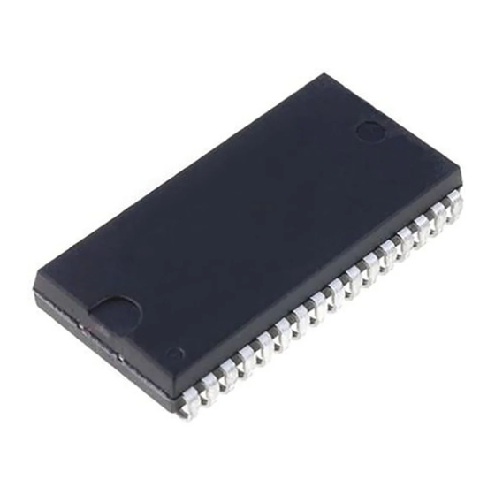
• Available in Pb-free 32-pin 300-Mil wide Molded SOJ
Logic Block Diagram
INPUTBUFFER
A
0
A
1
A
2
A
3
128K × 8
A
4
ARRAY
A
5
A
6
A
7
A
8
CE
COLUMN
WE
DECODER
OE
Note
1. For guidelines on SRAM system designs, please refer to the 'System Design Guidelines' Cypress application note, available on the internet at www.cypress.com.
Cypress Semiconductor Corporation
Document #: 38-05465 Rev. *D
Functional Description
The CY7C1018DV33 is a high-performance CMOS static
RAM organized as 131,072 words by 8 bits. Easy memory
expansion is provided by an active LOW Chip Enable (CE), an
active LOW Output Enable (OE), and tri-state drivers. This
device has an automatic power-down feature that significantly
reduces power consumption when deselected.
Writing to the device is accomplished by taking Chip Enable
(CE) and Write Enable (WE) inputs LOW. Data on the eight I/O
pins (I/O
specified on the address pins (A
Reading from the device is accomplished by taking Chip
Enable (CE) and Output Enable (OE) LOW while forcing Write
Enable (WE) HIGH. Under these conditions, the contents of
the memory location specified by the address pins will appear
on the I/O pins.
The eight input/output pins (I/O
high-impedance state when the device is deselected (CE
HIGH), the outputs are disabled (OE HIGH), or during a write
operation (CE LOW, and WE LOW).
The CY7C1018DV33 is available in Pb-free 32-pin 300-Mil
wide Molded SOJ.
POWER
DOWN
•
198 Champion Court
1-Mbit (128K x 8) Static RAM
[1]
through I/O
) is then written into the location
0
7
Pin Configuration
A
1
0
A
1
2
A
3
2
A
4
3
I/O
0
CE
5
I/O
6
0
I/O
1
I/O
7
1
V
I/O
8
CC
2
V
9
SS
I/O
I/O
10
3
2
I/O
11
3
I/O
WE
4
12
A
4
13
I/O
5
A
5
14
A
15
6
I/O
6
A
16
7
I/O
7
,
•
San Jose
CA 95134-1709
CY7C1018DV33
through A
).
0
16
through I/O
) are placed in a
0
7
SOJ
Top View
A
32
16
31
A
15
30
A
14
A
29
13
28
OE
27
I/O
7
26
I/O
6
25
V
SS
24
V
CC
23
I/O
5
22
I/O
4
A
21
12
A
20
11
A
19
10
A
18
9
17
A
8
•
408-943-2600
Revised November 8, 2006
[+] Feedback
Advertisement
Table of Contents

Summary of Contents for Cypress Semiconductor CY7C1018DV33
- Page 1 (CE HIGH), the outputs are disabled (OE HIGH), or during a write operation (CE LOW, and WE LOW). The CY7C1018DV33 is available in Pb-free 32-pin 300-Mil wide Molded SOJ. • 198 Champion Court •...
-
Page 2: Selection Guide
< V , f = f Max. V , CE > V – 0.3V, > V – 0.3V, or V < 0.3V, f = 0 CY7C1018DV33 Unit ... –0.3V to V + 0.3V Ambient Speed Temperature 3.3V ± 0.3V –40°C to +85°C 10 ns –10 (Industrial) - Page 3 Still Air, soldered on a 3 × 4.5 inch, four-layer printed circuit board 3.0V 30 pF* Rise Time: 1 V/ns High-Z characteristics: R 317Ω 3.3V OUTPUT 5 pF 351Ω CY7C1018DV33 Max. Unit 400-Mil Unit Wide SOJ °C/W 57.61 °C/W 40.53 ALL INPUT PULSES...
- Page 4 , and t HZCE LZCE HZOE LZOE HZWE and t HZWE CY7C1018DV33 Unit Max. µs is less than t for any given device. LZWE Page 4 of 9 [+] Feedback...
- Page 5 < 0.3V DATA RETENTION MODE 3.0V > [13, 14] DATA VALID > 50 µs or stable at V > 50 µs. to V CC(min.) CC(min.) CY7C1018DV33 Min. Max. Unit – 0.3V, 3.0V DATA VALID HZOE HZCE HIGH IMPEDANCE Page 5 of 9...
-
Page 6: Switching Waveforms
17. If CE goes HIGH simultaneously with WE going HIGH, the output remains in a high-impedance state. 18. During this period the I/Os are in the output state and input signals should not be applied. Document #: 38-05465 Rev. *D DATA VALID [16, 17] DATA VALID CY7C1018DV33 Page 6 of 9 [+] Feedback... -
Page 7: Truth Table
–I/O High-Z Data Out Data In High-Z Ordering Information Speed Ordering Code (ns) CY7C1018DV33-10VXI Please contact your local Cypress sales representative for availability of these parts. Document #: 38-05465 Rev. *D [11, 17] DATA VALID Mode Power-down Read Write Selected, Outputs Disabled... -
Page 8: Package Diagram
Cypress against all charges. PIN 1 I.D DIMENSIONS IN INCHES 0.330 0.292 0.340 LEAD COPLANARITY 0.004 MAX. 0.305 0.128 0.140 0.025 MIN. CY7C1018DV33 MIN. MAX. 0.006 0.012 0.260 0.275 51-85041-*A Page 8 of 9 [+] Feedback... - Page 9 Document History Page Document Title: CY7C1018DV33, 1-Mbit (128K x 8) Static RAM Document Number: 38-05465 REV. ECN NO. Issue Date 201560 See ECN 238471 See ECN 262950 See ECN 307598 See ECN 520647 See ECN Document #: 38-05465 Rev. *D Orig.

Need help?
Do you have a question about the CY7C1018DV33 and is the answer not in the manual?
Questions and answers