Table of Contents
Advertisement
Quick Links
www.ti.com
User's Guide
DS90UH928QEVM User's Guide
1 DS90UH928QEVM Introduction.............................................................................................................................................
Requirements........................................................................................................................................................2
1.3 DS90UH928QEVM Overview............................................................................................................................................
1.4 Typical Application.............................................................................................................................................................
Guide....................................................................................................................................................................3
2.1 Board Setup.......................................................................................................................................................................
3 Evaluation Hardware Overview.............................................................................................................................................
Overview..................................................................................................................................................................5
3.2 Power.................................................................................................................................................................................
3.4 FPD-Link III Interface.........................................................................................................................................................
3.5 CML Loop-thru Monitor Interface.......................................................................................................................................
3.6
Controller............................................................................................................................................................................6
Addressing................................................................................................................................................6
Interface......................................................................................................................................................6
3.9 Device Address, Reset and Mode Selection Inputs...........................................................................................................
3.9.2 Mode Selection Inputs (S2).........................................................................................................................................
3.9.3 I2C Address Select (IDx).............................................................................................................................................
3.9.4 MODE_SEL (S5).........................................................................................................................................................
3.10
Indicators..........................................................................................................................................................................7
3.11 Input/Output Connectors..................................................................................................................................................
Software...........................................................................................................................................................................8
4.1 Overview............................................................................................................................................................................
4.2 Installation..........................................................................................................................................................................
4.3
Usage.................................................................................................................................................................................9
Tab..........................................................................................................................................................13
4.3.2 Pattern Generator Tab...............................................................................................................................................
Tab.............................................................................................................................................................13
Tab..............................................................................................................................................................13
4.4
Troubleshooting................................................................................................................................................................13
Documentation........................................................................................................................................................15
6 Board Schematic..................................................................................................................................................................
7 Bill of Materials.....................................................................................................................................................................
Layers.....................................................................................................................................................25
9 Revision History...................................................................................................................................................................
Trademarks
All trademarks are the property of their respective owners.
SNLU131A - FEBRUARY 2013 - REVISED JUNE 2024
Submit Document Feedback
Table of Contents
Contents........................................................................................................................................2
Output..............................................................................................................................................5
(S1)..............................................................................................................................................7
Copyright © 2024 Texas Instruments Incorporated
Table of Contents
DS90UH928QEVM User's Guide
2
2
3
3
5
5
6
6
6
7
7
7
8
8
9
13
16
21
27
1
Advertisement
Table of Contents

Related Manuals for Texas Instruments DS90UH928QEVM


Summary of Contents for Texas Instruments DS90UH928QEVM
-
Page 1: Table Of Contents
7 Bill of Materials..................................8 Board Layout and Layers..............................25 9 Revision History................................... Trademarks All trademarks are the property of their respective owners. SNLU131A – FEBRUARY 2013 – REVISED JUNE 2024 DS90UH928QEVM User's Guide Submit Document Feedback Copyright © 2024 Texas Instruments Incorporated... -
Page 2: Ds90Uh928Qevm Introduction
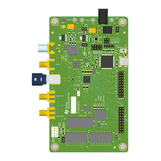
FPD-Link compatible LVDS data output pairs and one LVDS clock. The DS90UH928QEVM board features a 20-position IDC connector for connecting to the FPD-Link outputs, and a HSD Automotive Connector for connecting an automotive-grade STP cable to the FPD-Link III input. The included SMA connectors can also be configured as the FPD-Link III data input, enabling evaluation of other connectors and cable configurations. -
Page 3: Typical Application
1.8V position at JP10. 2. Connect an applicable cable (not provided, HSD automotive connector configured by default) from the DS90UH928QEVM (RX) board FPD-Link III input (J4) to the FPD-Link III output of a compatible FPD-Link III (TX) board (DS90UB925-Q1EVM or DS90UH927QEVM). - Page 4 Quick Start Guide www.ti.com Figure 2-1. DS90UB928-Q1EVM DS90UH928QEVM User's Guide SNLU131A – FEBRUARY 2013 – REVISED JUNE 2024 Submit Document Feedback Copyright © 2024 Texas Instruments Incorporated...
-
Page 5: Evaluation Hardware Overview
Check the specific target device or module to verify that proper LVDS termination is used. SNLU131A – FEBRUARY 2013 – REVISED JUNE 2024 DS90UH928QEVM User's Guide Submit Document Feedback Copyright © 2024 Texas Instruments Incorporated... -
Page 6: Fpd-Link Iii Interface
3.9 Device Address, Reset and Mode Selection Inputs The Mode Selection Inputs determine the specific mode or state of device operation. DS90UH928QEVM User's Guide SNLU131A – FEBRUARY 2013 – REVISED JUNE 2024 Submit Document Feedback Copyright © 2024 Texas Instruments Incorporated... -
Page 7: Output State Select (S1)
D2/LOCK Indicates LOCK status. The LED remains on if the link is active and the device is locked to the remote serializer. SNLU131A – FEBRUARY 2013 – REVISED JUNE 2024 DS90UH928QEVM User's Guide Submit Document Feedback Copyright © 2024 Texas Instruments Incorporated... -
Page 8: Input/Output Connectors
System Requirements: Operating system: Windows XP, Vista, or greater USB version: 2.0 DS90UH928QEVM User's Guide SNLU131A – FEBRUARY 2013 – REVISED JUNE 2024 Submit Document Feedback Copyright © 2024 Texas Instruments Incorporated... -
Page 9: Installation
MSP430 to communicate with the device. Users can find and install the program needed for this under MSP430USBDEVPACK/5.20.07.01, Python based Firmware Upgrade Example. To install the ALP hardware USB driver, connect the USB cable from the host PC to the DS90UH928QEVM USB port (J6): 1. - Page 10 ALP Software www.ti.com Figure 4-1. ALP Startup Screen Figure 4-2. Information Tab DS90UH928QEVM User's Guide SNLU131A – FEBRUARY 2013 – REVISED JUNE 2024 Submit Document Feedback Copyright © 2024 Texas Instruments Incorporated...
- Page 11 ALP Software Figure 4-3. Pattern Generator Tab Figure 4-4. Register Tab SNLU131A – FEBRUARY 2013 – REVISED JUNE 2024 DS90UH928QEVM User's Guide Submit Document Feedback Copyright © 2024 Texas Instruments Incorporated...
- Page 12 ALP Software www.ti.com Figure 4-5. Register Tab with expanded register description Figure 4-6. Scripting Tab DS90UH928QEVM User's Guide SNLU131A – FEBRUARY 2013 – REVISED JUNE 2024 Submit Document Feedback Copyright © 2024 Texas Instruments Incorporated...
-
Page 13: Information Tab
The USB driver is not installed. Check the device manager. There is a device named NSC ALP Nano Atmel device under the Universal Serial Bus Controllers as shown below. SNLU131A – FEBRUARY 2013 – REVISED JUNE 2024 DS90UH928QEVM User's Guide Submit Document Feedback Copyright © 2024 Texas Instruments Incorporated... - Page 14 After demo mode is disabled, the ALP software polls the ALP hardware. The ALP software updates and displays only DS90UH928Q under the Devices drop-down menu. DS90UH928QEVM User's Guide SNLU131A – FEBRUARY 2013 – REVISED JUNE 2024 Submit Document Feedback Copyright © 2024 Texas Instruments Incorporated...
-
Page 15: Related Documentation
TI Application Note: AN-2173 I2C Communication Over FPD-Link III with Bidirectional Control Channel (SNLA131) • TI Application Note: AN-2198 Exploring the Internal Test Pattern Generator Feature of 720p FPD-Link III Devices (SNLA132 SNLU131A – FEBRUARY 2013 – REVISED JUNE 2024 DS90UH928QEVM User's Guide Submit Document Feedback Copyright © 2024 Texas Instruments Incorporated... -
Page 16: Board Schematic
FP D3 INP UT S DA S ta tus LEDs CONNECTOR S CL PAS S UNLOCK MODE_SEL Figure 6-1. System Block Diagram DS90UH928QEVM User's Guide SNLU131A – FEBRUARY 2013 – REVISED JUNE 2024 Submit Document Feedback Copyright © 2024 Texas Instruments Incorporated... - Page 17 S CL S CL1 SCL1 100nF 4.7pF 4.7pF J P7 J P8 MODE_SEL MODE_SEL 100nF 100nF Figure 6-2. DS90UB928-Q1 Device SNLU131A – FEBRUARY 2013 – REVISED JUNE 2024 DS90UH928QEVM User's Guide Submit Document Feedback Copyright © 2024 Texas Instruments Incorporated...
- Page 18 AVCC1 AVS S 2 0.1uF 0.1uF DVCC1 DVS S 1 DVCC2 DVS S 2 MSP430F5529IPNR 100nF 100nF Figure 6-3. USB2ANY DS90UH928QEVM User's Guide SNLU131A – FEBRUARY 2013 – REVISED JUNE 2024 Submit Document Feedback Copyright © 2024 Texas Instruments Incorporated...
- Page 19 J 15 J P9 22uF 2.2uF 22uF 2.2uF 100nF VDD33C J P10 100nF VDD18C J 16 VDDIOC VDD33C Figure 6-4. Power SNLU131A – FEBRUARY 2013 – REVISED JUNE 2024 DS90UH928QEVM User's Guide Submit Document Feedback Copyright © 2024 Texas Instruments Incorporated...
- Page 20 The s e a s s e mblie s mus t comply with workma ns hip s ta nda rds IP C-A-610 Cla s s 2, unle s s othe rwis e s pe cifie d. De fa ult J umpe r P la ce me nt JP10 SH-J10 SH-JP10 SH-J9 SH-J13 Figure 6-5. Hardware DS90UH928QEVM User's Guide SNLU131A – FEBRUARY 2013 – REVISED JUNE 2024 Submit Document Feedback Copyright © 2024 Texas Instruments Incorporated...
-
Page 21: Bill Of Materials
Board Schematic 7 Bill of Materials Table 7-1. DS90UH928QEVM Bill of Materials Item Designator Part Number Quantity Manufacturer Package Reference Value C1, C2, C4, C5, C6, C9, GCM21BR71C475KA73L MuRata 0805 4.7uF C13, C14, C17, C18 GCM31CR70J226KE23L MuRata 1206 22uF... - Page 22 Board Schematic www.ti.com Table 7-1. DS90UH928QEVM Bill of Materials (continued) Item Designator Part Number Quantity Manufacturer Package Reference Value J2, J3, J6, J7 142-0701-851 Cinch Connectivity SMA End Launch D4S20D-40ML5-Z Rosenberger HSD connector, Waterblue J5, JP2 TSW-110-07-G-D Samtec 10x2 Header...
- Page 23 Board Schematic Table 7-1. DS90UH928QEVM Bill of Materials (continued) Item Designator Part Number Quantity Manufacturer Package Reference Value CRCW040212K4FKED Vishay-Dale 0402 12.4k CRCW040230K1FKED Vishay-Dale 0402 30.1k R39, R56 CRCW040221K0FKED Vishay-Dale 0402 21.0k R40, R55 CRCW040219K1FKED Vishay-Dale 0402 19.1k R41, R54...
- Page 24 Board Schematic www.ti.com Table 7-1. DS90UH928QEVM Bill of Materials (continued) Item Designator Part Number Quantity Manufacturer Package Reference Value KSR221GLFS C&K Components SH-J9, SH-J10, SH-J13, SNT-100-BK-G Samtec Shunt SH-JP10 ADTSM31NV APEM 6x3.51mm ACM9070-701-2PL-TL01 9x7mm Texas Instruments RHS0048A DS90UB928QSQX/NOPB LM2941LD/NOPB Texas Instruments...
-
Page 25: Board Layout And Layers
The following mechanical drawings (not to scale) illustrate the physical layout and stack-up of the 4-layer DS90UH928QEVM evaluation board: Figure 8-2. Top Layer Figure 8-1. Top Silkscreen SNLU131A – FEBRUARY 2013 – REVISED JUNE 2024 DS90UH928QEVM User's Guide Submit Document Feedback Copyright © 2024 Texas Instruments Incorporated... - Page 26 Board Layout and Layers www.ti.com Figure 8-3. Interal Layer 1: Signals Figure 8-4. Internal Layer 2: Signals 2 DS90UH928QEVM User's Guide SNLU131A – FEBRUARY 2013 – REVISED JUNE 2024 Submit Document Feedback Copyright © 2024 Texas Instruments Incorporated...
-
Page 27: Revision History
Changes from Revision * (February 2013) to Revision A (June 2024) Page • Updated document throughout to reflect hardware redesign................SNLU131A – FEBRUARY 2013 – REVISED JUNE 2024 DS90UH928QEVM User's Guide Submit Document Feedback Copyright © 2024 Texas Instruments Incorporated... - Page 28 STANDARD TERMS FOR EVALUATION MODULES Delivery: TI delivers TI evaluation boards, kits, or modules, including any accompanying demonstration software, components, and/or documentation which may be provided together or separately (collectively, an “EVM” or “EVMs”) to the User (“User”) in accordance with the terms set forth herein.
- Page 29 www.ti.com Regulatory Notices: 3.1 United States 3.1.1 Notice applicable to EVMs not FCC-Approved: FCC NOTICE: This kit is designed to allow product developers to evaluate electronic components, circuitry, or software associated with the kit to determine whether to incorporate such items in a finished product and software developers to write software applications for use with the end product.
- Page 30 www.ti.com Concernant les EVMs avec antennes détachables Conformément à la réglementation d'Industrie Canada, le présent émetteur radio peut fonctionner avec une antenne d'un type et d'un gain maximal (ou inférieur) approuvé pour l'émetteur par Industrie Canada. Dans le but de réduire les risques de brouillage radioélectrique à...
- Page 31 www.ti.com EVM Use Restrictions and Warnings: 4.1 EVMS ARE NOT FOR USE IN FUNCTIONAL SAFETY AND/OR SAFETY CRITICAL EVALUATIONS, INCLUDING BUT NOT LIMITED TO EVALUATIONS OF LIFE SUPPORT APPLICATIONS. 4.2 User must read and apply the user guide and other available documentation provided by TI regarding the EVM prior to handling or using the EVM, including without limitation any warning or restriction notices.
- Page 32 Notwithstanding the foregoing, any judgment may be enforced in any United States or foreign court, and TI may seek injunctive relief in any United States or foreign court. Mailing Address: Texas Instruments, Post Office Box 655303, Dallas, Texas 75265 Copyright © 2023, Texas Instruments Incorporated...
- Page 33 TI products. TI’s provision of these resources does not expand or otherwise alter TI’s applicable warranties or warranty disclaimers for TI products. TI objects to and rejects any additional or different terms you may have proposed. IMPORTANT NOTICE Mailing Address: Texas Instruments, Post Office Box 655303, Dallas, Texas 75265 Copyright © 2024, Texas Instruments Incorporated...
Need help?
Do you have a question about the DS90UH928QEVM and is the answer not in the manual?
Questions and answers