Advertisement
Features
• Pin- and function-compatible with CY7C1018BV33
• High speed
— t
= 10 ns
AA
• CMOS for optimum speed/power
• Center power/ground pinout
• Data retention at 2.0V
• Automatic power-down when deselected
• Easy memory expansion with CE and OE options
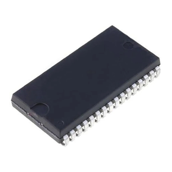
• Available in Pb-free and non Pb-free 300-mil-wide
32-pin SOJ
Functional Description
The CY7C1018CV33 is a high-performance CMOS static
RAM organized as 131,072 words by 8 bits. Easy memory
expansion is provided by an active LOW Chip Enable (CE), an
active LOW Output Enable (OE), and tri-state drivers. This
Logic Block Diagram
INPUT BUFFER
A
0
A
1
A
2
A
3
A
4
128K x 8
A
5
ARRAY
A
6
A
7
A
8
COLUMN
CE
DECODER
WE
OE
Note:
1.
For guidelines on SRAM system designs, please refer to the 'System Design Guidelines' Cypress application note, available on the internet at www.cypress.com.
Cypress Semiconductor Corporation
Document #: 38-05131 Rev. *D
[1]
POWER
DOWN
•
198 Champion Court
128K x 8 Static RAM
device has an automatic power-down feature that significantly
reduces power consumption when deselected.
Writing to the device is accomplished by taking Chip Enable
(CE) and Write Enable (WE) inputs LOW. Data on the eight I/O
pins (I/O
through I/O
) is then written into the location
0
7
specified on the address pins (A
Reading from the device is accomplished by taking Chip
Enable (CE) and Output Enable (OE) LOW while forcing Write
Enable (WE) HIGH. Under these conditions, the contents of
the memory location specified by the address pins will appear
on the I/O pins.
The eight input/output pins (I/O
high-impedance state when the device is deselected (CE
HIGH), the outputs are disabled (OE HIGH), or during a write
operation (CE LOW, and WE LOW).
The CY7C1018CV33 is available in a standard 300-mil-wide
SOJ.
Pin Configurations
Top View
A
1
0
A
1
2
A
3
2
A
4
3
I/O
0
CE
5
I/O
6
0
I/O
1
I/O
7
1
V
8
CC
I/O
2
V
9
SS
I/O
10
2
I/O
3
I/O
11
3
WE
12
I/O
4
A
4
13
A
5
14
I/O
5
A
15
6
A
16
7
I/O
6
I/O
7
,
•
San Jose
CA 95134-1709
CY7C1018CV33
through A
).
0
16
through I/O
) are placed in a
0
7
SOJ
A
32
16
31
A
15
30
A
14
A
29
13
28
OE
27
I/O
7
26
I/O
6
25
V
SS
24
V
CC
23
I/O
5
22
I/O
4
A
21
12
A
20
11
A
19
10
A
18
9
A
17
8
•
408-943-2600
Revised August 3, 2006
[+] Feedback
Advertisement
Table of Contents

Summary of Contents for Cypress Semiconductor CY7C1018CV33
- Page 1 The eight input/output pins (I/O high-impedance state when the device is deselected (CE HIGH), the outputs are disabled (OE HIGH), or during a write operation (CE LOW, and WE LOW). The CY7C1018CV33 is available in a standard 300-mil-wide SOJ. POWER DOWN •...
-
Page 2: Selection Guide
, f = f Comm’l – 0.3V, Ind’l – 0.3V, < 0.3V, f = 0 Test Conditions = 25°C, f = 1 MHz, = 3.3V CY7C1018CV33 Unit Ambient Temperature 3.3V ± 10% 0°C to +70°C 3.3V ± 10% –40°C to +85°C –12 –15 Min. - Page 3 Min. is less than t is less than t , and t HZCE LZCE HZOE LZOE HZWE HZWE CY7C1018CV33 Fall Time: 1 V/ns Max. Min. Max. Unit is less than t for any given device. LZWE and t Page 3 of 7...
- Page 4 14. Data I/O is high impedance if OE = V 15. If CE goes HIGH simultaneously with WE going HIGH, the output remains in a high-impedance state. Document #: 38-05131 Rev. *D DATA VALID DATA VALID CY7C1018CV33 DATA VALID HZOE HZCE HIGH...
- Page 5 16. During this period the I/Os are in the output state and input signals should not be applied. Document #: 38-05131 Rev. *D [14, 15] DATA VALID [10, 15] DATA VALID Mode Power-down Read Write Selected, Outputs Disabled CY7C1018CV33 LZWE Power Standby (I Active (I Active (I Active (I Page 5 of 7 [+] Feedback...
-
Page 6: Ordering Information
Ordering Information Speed (ns) Ordering Code CY7C1018CV33-10VC CY7C1018CV33-12VC CY7C1018CV33-12VXI CY7C1018CV33-15VXC Package Diagram All product and company names mentioned in this document are the trademarks of their respective holders. Document #: 38-05131 Rev. *D © Cypress Semiconductor Corporation, 2006. The information contained herein is subject to change without notice. Cypress Semiconductor Corporation assumes no responsibility for the use of any circuitry other than circuitry embodied in a Cypress product. - Page 7 Document History Page Document Title: CY7C1018CV33 128K x 8 Static RAM Document Number: 38-05131 Issue REV. ECN NO. Date 109426 12/14/01 113432 04/10/02 115046 05/30/02 116476 09/16/02 493543 See ECN Document #: 38-05131 Rev. *D Orig. of Change Description of Change...

Need help?
Do you have a question about the CY7C1018CV33 and is the answer not in the manual?
Questions and answers