Table of Contents
Advertisement
Quick Links
Features
■
High speed
❐
t
= 10 ns
AA
■
Low active power
❐
I
= 175 mA at 10 ns
CC
■
Low CMOS standby power
❐
I
= 25 mA
SB2
■
Operating voltages of 3.3 ± 0.3V
■
2.0V data retention
■
Automatic power down when deselected
■
TTL compatible inputs and outputs
■
Available in Pb-free standard 119-ball PBGA
Logic Block Diagram
A
(9:0)
Cypress Semiconductor Corporation
Document Number: 38-05610 Rev. *D
Functional Description
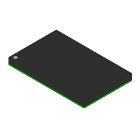
The CY7C1012DV33 is a high performance CMOS static RAM
organized as 512K words by 24 bits. Each data byte is separately
controlled by the individual chip selects (CE
CE
1
data on I/O
I/O
16
that significantly reduces power consumption when deselected.
Writing the data bytes into the SRAM is accomplished when the
chip select controlling that byte is LOW and the write enable input
(WE) input is LOW. Data on the respective input and output (I/O)
pins is then written into the location specified on the address pins
(A
– A
0
LOW writes all 24 bits of data into the SRAM. Output enable (OE)
is ignored while in WRITE mode.
Data bytes are also individually read from the device. Reading a
byte is accomplished when the chip select controlling that byte
is LOW and write enable (WE) HIGH, while output enable (OE)
remains LOW. Under these conditions, the contents of the
memory location specified on the address pins appear on the
specified data input and output (I/O) pins. Asserting all the chip
selects LOW reads all 24 bits of data from the SRAM.
The 24 I/O pins (I/O
state when all the chip selects are HIGH or when the output
enable (OE) is HIGH during a READ mode. For more infor-
mation, see the
INPUT BUFFER
512K x 24
ARRAY
COLUMN
DECODER
CONTROL LOGIC
A
(18:10)
•
198 Champion Court
12-Mbit (512K X 24) Static RAM
controls the data on the I/O
– I/O
0
– I/O
, and CE
controls the data on the data pins
8
15
3
– I/O
. This device has an automatic power down feature
23
). Asserting all of the chip selects LOW and write enable
18
– I/O
) are placed in a high impedance
0
23
Truth Table
on page 8.
I/O
– I/O
0
7
I/O
– I/O
8
15
I/O
– I/O
16
CE
, CE
, CE
1
2
3
WE
OE
,
•
San Jose
CA 95134-1709
CY7C1012DV33
, CE
, and CE
).
1
2
3
, while CE
controls the
7
2
23
•
408-943-2600
Revised November 6, 2008
[+] Feedback
Advertisement
Table of Contents

Summary of Contents for Cypress Semiconductor CY7C1012DV33
-
Page 1: Functional Description
Document Number: 38-05610 Rev. *D 12-Mbit (512K X 24) Static RAM Functional Description The CY7C1012DV33 is a high performance CMOS static RAM organized as 512K words by 24 bits. Each data byte is separately controlled by the individual chip selects (CE... -
Page 2: Selection Guide
Maximum Operating Current Maximum CMOS Standby Current Pin Configuration Note 1. NC pins are not connected on the die. Document Number: 38-05610 Rev. *D Figure 1. 119-Ball PBGA ( Top View) CY7C1012DV33 –10 Unit Page 2 of 11 [+] Feedback... -
Page 3: Maximum Ratings
< V , f = f Max V , CE > V – 0.3V, > V – 0.3V, or V < 0.3V, f = 0 or CE CY7C1012DV33 Ambient Temperature 3.3V ± 0.3V –40°C to +85°C –10 + 0.3 –0.3 –1 –1... -
Page 4: Thermal Resistance
Still air, soldered on a 3 × 4.5 inch, four layer printed circuit board Figure 2. AC Test Loads and Waveforms = 1.5V All input pulses 3.0V to the data retention (V , 2.0V) voltage. CCDR CY7C1012DV33 Unit 119-Ball Unit PBGA °C/W 20.31 °C/W 8.35 R1 317 Ω... - Page 5 CE or CE LOW and WE LOW. Chip enables must be active and WE must be LOW to initiate and t HZWE CY7C1012DV33 –10 Unit μs 2. Transition is measured ±200 mV from steady state Page 5 of 11...
-
Page 6: Switching Waveforms
[13, 14] Figure 3. Read Cycle No. 1 LZOE DATA VALID > 50 μs or stable at V > 50 μs. to V CC(min) CC(min) CY7C1012DV33 Unit 3.0V DATA VALID [3, 14, 15] HZOE HZCE HIGH IMPEDANCE Page 6 of 11... - Page 7 18. During this period, the I/Os are in output state. Do not apply input signals. Document Number: 38-05610 Rev. *D DATA VALID DATA VALID DATA VALID CY7C1012DV33 [3, 16, 17] [3, 16, 17] [3, 17] LZWE Page 7 of 11...
-
Page 8: Truth Table
Data In High Z High Z High Z Data In Full Data In Full Data In Full Data In High Z High Z High Z CY7C1012DV33 Mode Power Power Down Standby (I Read Active (I Read Active (I Read Active (I... -
Page 9: Ordering Information
CY7C1012DV33 Ordering Information Speed Package Operating Ordering Code Package Type (ns) Name Range CY7C1012DV33-10BGXI 51-85115 119-Ball Plastic Ball Grid Array (14 x 22 x 2.4 mm) (Pb-Free) Industrial Package Diagram Figure 8. 119-Ball PBGA (14 x 22 x 2.4 mm) 51-85115-*B Document Number: 38-05610 Rev. - Page 10 Document History Page Document Title: CY7C1012DV33 12-Mbit (512K X 24) Static RAM Document Number: 38-05610 Orig. of Submission Rev. ECN No. Change Date 250650 See ECN 469517 See ECN 499604 See ECN 1462585 See ECN 2604677 VKN/PYRS 11/12/08 Document Number: 38-05610 Rev. *D...
- Page 11 All product and company names mentioned in this document are the trademarks of their respective holders PSoC Solutions psoc.cypress.com General clocks.cypress.com Low Power/Low Voltage Precision Analog LCD Drive image.cypress.com CAN 2.0b Revised November 6, 2008 CY7C1012DV33 psoc.cypress.com/solutions psoc.cypress.com/low-power psoc.cypress.com/precision-analog psoc.cypress.com/lcd-drive psoc.cypress.com/can psoc.cypress.com/usb Page 11 of 11 [+] Feedback...

Need help?
Do you have a question about the CY7C1012DV33 and is the answer not in the manual?
Questions and answers