Table of Contents
Advertisement
Quick Links
Features
■
25 ns, 35 ns, and 45 ns access times
■
Pin compatible with STK17T88
■
Data integrity of Cypress nvSRAM combined with full featured
Real Time Clock
❐
Low power, 350 nA RTC current
❐
Capacitor or battery backup for RTC
■
Watchdog timer
■
Clock alarm with programmable interrupts
■
Hands off automatic STORE on power down with only a small
capacitor
■
STORE to QuantumTrap™ initiated by software, device pin, or
on power down
■
RECALL to SRAM initiated by software or on power up
■
Infinite READ, WRITE, and RECALL cycles
Logic Block Diagram
A
5
A
6
A
7
A
8
A
9
A
11
A
12
A
13
A
14
DQ
0
DQ
1
DQ
2
DQ
3
DQ
4
DQ
5
DQ
6
DQ
7
Cypress Semiconductor Corporation
Document Number: 001-06431 Rev. *H
256 Kbit (32K x 8) nvSRAM with Real Time Clock
■
High reliability
❐
❐
■
Single 3V operation with tolerance of +20%, -10%
■
Commercial and industrial temperature
■
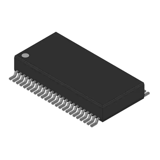
48-Pin SSOP (ROHS compliant)
Functional Description
The Cypress CY14B256K combines a 256 Kbit nonvolatile static
RAM with a full-featured real time clock in a monolithic integrated
circuit. The embedded nonvolatile elements incorporate
QuantumTrap technology producing the world's most reliable
nonvolatile memory. The SRAM is read and written an infinite
number of times, while independent, nonvolatile data resides in
the nonvolatile elements.
The real time clock function provides an accurate clock with leap
year tracking and a programmable high accuracy oscillator. The
alarm function is programmable for one time alarms or periodic
seconds, minutes, hours, or days. There is also a programmable
watchdog timer for process control.
QuantumTrap
512 X 512
STORE
RECALL
STATIC RAM
ARRAY
512 X 512
COLUMN IO
COLUMN DEC
A
A
A
A
A
A
0
1
2
3
4
10
•
198 Champion Court
Endurance to 200K cycles
Data retention: 20 years at 55°C
V
V
CC
CAP
V
RTCbat
POWER
CONTROL
V
RTCcap
STORE/
RECALL
CONTROL
SOFTWARE
DETECT
RTC
MUX
,
•
San Jose
CA 95134-1709
CY14B256K
HSB
-
A
A
13
0
x
1
x
2
INT
-
A
A
14
0
OE
CE
WE
•
408-943-2600
Revised February 24, 2009
[+] Feedback
Advertisement
Table of Contents

Subscribe to Our Youtube Channel
Related Manuals for Cypress Semiconductor CY14B256K


Summary of Contents for Cypress Semiconductor CY14B256K
-
Page 1: Functional Description
■ 48-Pin SSOP (ROHS compliant) Functional Description The Cypress CY14B256K combines a 256 Kbit nonvolatile static RAM with a full-featured real time clock in a monolithic integrated circuit. The embedded nonvolatile elements incorporate QuantumTrap technology producing the world’s most reliable nonvolatile memory. -
Page 2: Pin Configurations
Power Supply AutoStore Capacitor. Supplies power to nvSRAM during power loss to store data from SRAM to nonvolatile elements. Document Number: 001-06431 Rev. *H Figure 1. 48-Pin SSOP 48-SSOP Top View (Not To Scale) Description CY14B256K RTCcap is used) RTCbat is used) RTCcap Page 2 of 28 [+] Feedback... -
Page 3: Device Operation
LOW, internal circuitry turns off the output buffers t goes LOW. ® AutoStore Operation The CY14B256K stores data to nvSRAM using one of the three storage operations: 1. Hardware store activated by HSB 2. Software store activated by an address sequence 3. AutoStore on device power down AutoStore operation is a unique feature of QuantumTrap technology and is enabled by default on the CY14B256K. - Page 4 V is less than V If the CY14B256K is in a WRITE mode (both CE and WE are low) at power up after a RECALL, or after a STORE, the WRITE is inhibited until a negative transition on CE or WE is detected. This protects against inadvertent writes during power up or brown out conditions.
- Page 5 V 3.6V, and chip enable at maximum frequency. Only standby current is drawn when the chip is disabled. The overall average current drawn by the CY14B256K depends on the following items: 1. 1The duty cycle of chip enable 2.
- Page 6 1. The six consecutive address locations are in the order listed. WE is HIGH during all six cycles to enable a nonvolatile cycle. 2. While there are 15 address lines on the CY14B256K, only the lower 14 lines are used to control software modes.
-
Page 7: Real Time Clock Operation
The battery is not, however, recharged at any time by the CY14B256K. The battery capacity must be chosen for total antic- ipated cumulative down time required over the life of the system. - Page 8 32.768 kHz. Clock accuracy depends on the quality of the crystal and calibration. The crystal oscillators typically have an error of +20ppm to +35ppm. However, CY14B256K employs a calibration circuit that improves the accuracy to +1/–2 ppm at 25°C. This implies an error of +2.5 seconds to -5 seconds per month.
- Page 9 “AutoStore or Power Up RECALL” on page 19). Interrupts The CY14B256K has a Flags register, Interrupt register and Interrupt logic that can signal interrupt to the microcontroller. There are three potential sources for interrupt: watchdog timer, power monitor, and alarm timer. Each of these can be individually enabled to drive the INT pin by appropriate setting in the Interrupt register (0x7FF6).
- Page 10 Document Number: 001-06431 Rev. *H Figure 5. Interrupt Block Diagram Driver and DQ in applications where undershoot exceeds -0.5V. Please see CY14B256K WDF - Watchdog Timer Flag WIE - Watchdog Interrupt Enable PF - Power Fail Flag PFE - Power Fail Enable...
- Page 11 WDT (000000) H/L (1) P/L (0) Alarm Day Alarm Hours Alarm Minutes Alarm, Seconds Centuries OSCF CAL (0) CY14B256K Function/Range Years: 00–99 Months: 01–12 Day of Month: 01–31 Day of Week: 01–07 Hours: 00–23 Minutes: 00–59 Seconds: 00–59 Calibration Values...
- Page 12 10s Day of Month Time Keeping - Day Time Keeping - Hours 10s Hours Time Keeping - Minutes 10s Minutes Time Keeping - Seconds 10s Seconds CY14B256K Years Months Day of Month Day of Week Hours Minutes Seconds Page 12 of 28...
- Page 13 Match. When this bit is set to 0, the date value is used in the alarm match. Setting this bit to 1 causes the match circuit to ignore the date value. Document Number: 001-06431 Rev. *H Calibration/Control Calibration Sign WatchDog Timer Interrupt Status/Control PFIE Alarm - Day 10s Alarm Date CY14B256K Calibration “Watchdog Alarm Date Page 13 of 28 [+] Feedback...
- Page 14 Document Number: 001-06431 Rev. *H Alarm - Hours 10s Alarm Hours Alarm - Minutes Alarm - Seconds Time Keeping - Centuries Flags OSCF CY14B256K Alarm Hours Alarm Minutes Alarm Seconds Centuries . It is cleared to SWITCH Page 14 of 28...
-
Page 15: Maximum Ratings
< V < V , CE or OE > V = –2 mA = 4 mA pin and V , 5V Rated CY14B256K = 25°C) ... 1.0W Ambient Temperature 0°C to +70°C 2.7V to 3.6V –40°C to +85°C 2.7V to 3.6V... -
Page 16: Thermal Resistance
Test Conditions Test conditions follow standard test methods and procedures for measuring thermal impedance, in accordance with EIA / JESD51. Figure 7. AC Test Loads 3.0V Output 5 pF 789Ω CY14B256K Unit Years Unit 48-SSOP Unit °C/W 32.9 °C/W 25.56 R1 577Ω... - Page 17 13. These parameters are guaranteed by design and are not tested. 14. HSB must remain HIGH during READ and WRITE cycles. Document Number: 001-06431 Rev. *H 25 ns Description CY14B256K 35 ns 45 ns Unit [10, 11, 14] [10, 14]...
- Page 18 Document Number: 001-06431 Rev. *H (continued) 25 ns Description DATA VALID HZWE HIGH IMPEDANCE Figure 11. SRAM Write Cycle 2: CE Controlled DATA VALID HIGH IMPEDANCE CY14B256K 35 ns 45 ns Unit [14, 16] LZWE Page 18 of 28 [+] Feedback...
- Page 19 18. If an SRAM Write does not taken place since the last nonvolatile cycle, no STORE takes place. 19. Industrial Grade Devices require 15 ms Max. Document Number: 001-06431 Rev. *H Commercial Industrial Figure 12. AutoStore/Power Up RECALL STORE HRECALL SWITCH CY14B256K CY14B256K Unit 12.5 2.65 μs STORE occurs only No STORE occurs if a SRAM write...
- Page 20 21. The six consecutive addresses are read in the order listed in the Document Number: 001-06431 Rev. *H [20, 21] 25 ns DATA VALID DATA VALID Mode Selection on page 6. WE is HIGH during all six consecutive cycles. CY14B256K 35 ns 45 ns [21] STORE RECALL HIGH IMPEDANCE [21]...
- Page 21 24. Commands such as STORE and RECALL lock out IO until operation is complete which further increases this time. See specific command. Document Number: 001-06431 Rev. *H Description Figure 15. Hardware STORE Cycle Figure 16. Soft Sequence Processing CY14B256K CY14B256K Unit μs CY14B256K Unit μs...
- Page 22 27. Typical = 2.4V during normal operation. Document Number: 001-06431 Rev. *H Test Conditions At 25°C Temperature from Power up or Enable Mode Deselect/Power down –DQ Read Output Disabled –DQ Write CY14B256K Unit Commercial Industrial Power Standby Active Active Active Page 22 of 28 [+] Feedback...
-
Page 23: Part Numbering Nomenclature
I - Industrial (–40 to 85°C) Package: SP - 48-SSOP Data Bus: K - x8 + RTC Voltage: B - 3.0V CY14B256K Speed: 25 - 25 ns 35 - 35 ns 45 - 45 ns Density: 256 - 256 Kb... -
Page 24: Ordering Information
Ordering Information All the below mentioned parts are Pb-free. Contact your local Cypress sales representative for availability of these parts. Speed (ns) Ordering Code CY14B256K-SP25XC CY14B256K-SP25XCT CY14B256K-SP25XI CY14B256K-SP25XIT CY14B256K-SP35XC CY14B256K-SP35XCT CY14B256K-SP35XI CY14B256K-SP35XIT CY14B256K-SP45XC CY14B256K-SP45XCT CY14B256K-SP45XI CY14B256K-SP45XIT Document Number: 001-06431 Rev. *H... -
Page 25: Package Diagrams
CY14B256K Package Diagrams Figure 17. 48-Pin Shrunk Small Outline Package (51-85061) 51-85061-*C Document Number: 001-06431 Rev. *H Page 25 of 28 [+] Feedback... - Page 26 Document History Page Document Title: CY14B256K 256 Kbit (32K x 8) nvSRAM with Real Time Clock Document Number: 001-06431 Rev. Orig. of Change 425138 437321 471966 503277 597004 696097 1349963 UHA/SFV 2483006 GVCH/PYRS Document Number: 001-06431 Rev. *H Submission Description of Change...
- Page 27 Document Title: CY14B256K 256 Kbit (32K x 8) nvSRAM with Real Time Clock Document Number: 001-06431 Rev. Orig. of Change 2663934 GVCH/PYRS Document Number: 001-06431 Rev. *H Submission Description of Change Date 02/24/09 Updated Features section Updated pin definition of WE pin Updated “Reading the clock”, “Backup Power”, “Stopping and...
- Page 28 All products and company names mentioned in this document are the trademarks of their respective holders. PSoC Solutions psoc.cypress.com General clocks.cypress.com Low Power/Low Voltage Precision Analog LCD Drive image.cypress.com CAN 2.0b Revised February 24, 2009 CY14B256K psoc.cypress.com/solutions psoc.cypress.com/low-power psoc.cypress.com/precision-analog psoc.cypress.com/lcd-drive psoc.cypress.com/can psoc.cypress.com/usb Page 28 of 28 [+] Feedback...
Need help?
Do you have a question about the CY14B256K and is the answer not in the manual?
Questions and answers