Table of Contents
Advertisement
Quick Links
Features
• Very high speed: 45 ns
• Voltage range: 4.5V–5.5V
• Pin compatible with CY62148B
• Ultra low standby power
— Typical standby current: 1 µA
— Maximum standby current: 7 µA (Industrial)
• Ultra low active power
— Typical active current: 2.0 mA @ f = 1 MHz
• Easy memory expansion with CE, and OE features
• Automatic power down when deselected
• CMOS for optimum speed and power
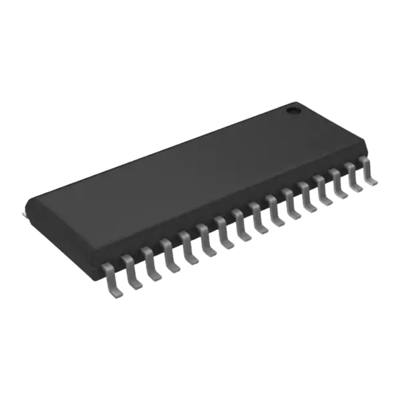
• Available in Pb-free 32-pin TSOP II and 32-pin SOIC
packages
Product Portfolio
Product
Range
CY62148ELL
TSOP II
CY62148ELL
SOIC
Ind'l/Auto-A
Notes
1. For best practice recommendations, refer to the Cypress application note "System Design Guidelines" at http://www.cypress.com.
2. SOIC package is available only in 55 ns speed bin.
3. Typical values are included for reference only and are not guaranteed or tested. Typical values are measured at V
Cypress Semiconductor Corporation
Document #: 38-05442 Rev. *F
[2]
V
Range (V)
CC
[3]
Min
Typ
Ind'l
4.5
5.0
4.5
5.0
•
198 Champion Court
4-Mbit (512K x 8) Static RAM
Functional Description
The CY62148E is a high performance CMOS static RAM
organized as 512K words by 8 bits. This device features
advanced circuit design to provide ultra low active current.
This is ideal for providing More Battery Life™ (MoBL
portable applications such as cellular telephones. The device
also has an automatic power down feature that significantly
reduces power consumption when addresses are not toggling.
Placing the device into standby mode reduces power
consumption by more than 99% when deselected (CE HIGH).
The eight input and output pins (IO
in a high impedance state when:
• Deselected (CE HIGH)
• Outputs are disabled (OE HIGH)
• Write operation is active (CE LOW and WE LOW)
To write to the device, take Chip Enable (CE) and Write Enable
(WE) inputs LOW. Data on the eight IO pins (IO
is then written into the location specified on the address pins
(A
through A
).
0
18
To read from the device, take Chip Enable (CE) and Output
Enable (OE) LOW while forcing Write Enable (WE) HIGH.
Under these conditions, the contents of the memory location
specified by the address pins appear on the IO pins.
Speed
Operating I
(ns)
f = 1MHz
[3]
Max
Typ
Max
5.5
45
2
2.5
5.5
55
2
2.5
,
•
San Jose
CA 95134-1709
CY62148E MoBL
[1]
through IO
) are placed
0
7
through IO
0
Power Dissipation
(mA)
CC
Standby I
SB2
f = f
max
[3]
[3]
Typ
Max
Typ
Max
15
20
1
15
20
1
= V
, T
= 25°C.
CC
CC(typ)
A
•
408-943-2600
Revised March 28, 2007
®
®
) in
)
7
(µA)
7
7
[+] Feedback
Advertisement
Table of Contents

Related Manuals for Cypress Semiconductor CY62148E


Summary of Contents for Cypress Semiconductor CY62148E
- Page 1 Document #: 38-05442 Rev. *F 4-Mbit (512K x 8) Static RAM Functional Description The CY62148E is a high performance CMOS static RAM organized as 512K words by 8 bits. This device features advanced circuit design to provide ultra low active current.
-
Page 2: Logic Block Diagram
Document #: 38-05442 Rev. *F INPUT BUFFER 512K x 8 ARRAY POWER COLUMN DECODER DOWN 32-pin SOIC/TSOP II Pinout Top View ® CY62148E MoBL IO 0 IO 1 IO 2 IO 3 IO 4 IO 5 IO 6 IO 7 Page 2 of 10... -
Page 3: Maximum Ratings
< 0.2V, CC(max) Test Conditions = 25°C, f = 1 MHz, CC(typ) (min) and 200 µs wait time after V spec. Other inputs can be left floating. CY62148E MoBL [5, 6] ... –0.5V to 6.0V (V + 0.5V) CCmax Ambient Temperature –40°C to +85°C... - Page 4 < 0.2V DATA RETENTION MODE > 2.0V CC(min) > 100 µs or stable at V > 100 µs. to V CC(min) CC(min) ® CY62148E MoBL SOIC TSOP II Unit Package Package °C/W °C/W Fall Time = 1 V/ns Unit Ω...
-
Page 5: Switching Characteristics
, and t HZCE LZCE HZOE LZOE . All signals must be ACTIVE to initiate a write and any of these signals can ® CY62148E MoBL 55 ns Unit is less than t for any given device. HZWE LZWE Page 5 of 10... -
Page 6: Switching Waveforms
21. During this period, the IOs are in output state and input signals must not be applied. Document #: 38-05442 Rev. *F [16, 17] DATA VALID [19, 20] DATA VALID ® CY62148E MoBL DATA VALID HZOE HZCE HIGH IMPEDANCE Page 6 of 10... -
Page 7: Truth Table
High Z Document #: 38-05442 Rev. *F DATA VALID [20] DATA VALID IO’s Mode Deselect/Power down Read Write Selected, Outputs Disabled ® CY62148E MoBL LZWE Power Standby (I Active (I Active (I Active (I Page 7 of 10 [+] Feedback... -
Page 8: Ordering Information
Document #: 38-05442 Rev. *F Package Package Type Diagram 51-85095 32-pin Thin Small Outline Package II (Pb-free) 51-85081 32-pin Small Outline Integrated Circuit (Pb-free) 51-85081 32-pin Small Outline Integrated Circuit (Pb-free) ® CY62148E MoBL Operating Range Industrial Industrial Automotive-A 51-85095-** Page 8 of 10... - Page 9 Cypress against all charges. 0.546[13.868] 0.566[14.376] 0.440[11.176] 0.450[11.430] 0.006[0.152] 0.012[0.304] 0.118[2.997] MAX. 0.004[0.102] 0.004[0.102] MIN. SEATING PLANE ® CY62148E MoBL 0.047[1.193] 0.063[1.600] 0.023[0.584] 0.039[0.990] 51-85081-*B Page 9 of 10 [+] Feedback...
- Page 10 Changed the address of Cypress Semiconductor Corporation on Page #1 from “3901 North First Street” to “198 Champion Court” Removed 35ns Speed Bin Removed “L” version of CY62148E Changed I (Typ) value from 1.5 mA to 2 mA at f=1 MHz Changed I (Max) value from 2 mA to 2.5 mA at f=1 MHz...
Need help?
Do you have a question about the CY62148E and is the answer not in the manual?
Questions and answers