Table of Contents
Advertisement
Quick Links
Features
• High speed: 55 ns and 70 ns
• Voltage range: 4.5V–5.5V operation
• Low active power (70 ns, LL version)
— 275 mW (max.)
• Low standby power (70 ns, LL version)
— 28 W (max.)
• Easy memory expansion with CE and OE features
• TTL-compatible inputs and outputs
• Automatic power-down when deselected
• CMOS for optimum speed/power
• Package available in a standard 450-mil-wide (300-mil
body width) 28-lead narrow SOIC, 28-lead TSOP-1,
28-lead reverse TSOP-1, and 600-mil 28-lead PDIP
packages
Logic Block Diagram
Note:
1.
For best practice recommendations, please refer to the Cypress application note "System Design Guidelines" on http://www.cypress.com.
Cypress Semiconductor Corporation
Document #: 38-05248 Rev. *B
INPUTBUFFER
A
10
A
9
A
8
A
7
A
6
512 x 512
A
5
ARRA Y
A
4
A
3
A
2
CE
WE
COLUMN
DECODER
OE
•
3901 North First Street
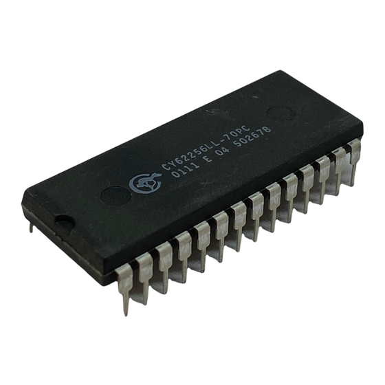
256K (32K x 8) Static RAM
Functional Description
The CY62256 is a high-performance CMOS static RAM
organized as 32K words by 8 bits. Easy memory expansion is
provided by an active LOW chip enable (CE) and active LOW
output enable (OE) and three-state drivers. This device has an
automatic
power-down
consumption by 99.9% when deselected.
An active LOW write enable signal (WE) controls the
writing/reading operation of the memory. When CE and WE
inputs are both LOW, data on the eight data input/output pins
(I/O
through I/O
) is written into the memory location
0
7
addressed by the address present on the address pins (A
through A
). Reading the device is accomplished by selecting
14
the device and enabling the outputs, CE and OE active LOW,
while WE remains inactive or HIGH. Under these conditions,
the contents of the location addressed by the information on
address pins are present on the eight data input/output pins.
The input/output pins remain in a high-impedance state unless
the chip is selected, outputs are enabled, and write enable
(WE) is HIGH.
POWER
DOWN
•
San Jose
•
CY62256
[1]
feature,
reducing
the
I/O
0
I/O
1
I/O
2
I/O
3
I/O
4
I/O
5
I/O
6
I/O
7
CA 95134
•
408-943-2600
Revised August 27, 2002
power
0
Advertisement
Table of Contents

Related Manuals for Cypress 256K (32K x 8) CY62256


Summary of Contents for Cypress 256K (32K x 8) CY62256
- Page 1 Features • High speed: 55 ns and 70 ns • Voltage range: 4.5V–5.5V operation • Low active power (70 ns, LL version) — 275 mW (max.) • Low standby power (70 ns, LL version) — 28 W (max.) • Easy memory expansion with CE and OE features •...
-
Page 2: Pin Configurations
Pin Configurations Narrow SOIC Top View V CC A 10 A 11 A 12 A 13 A 14 I/O 7 I/O 6 I/O 0 I/O 5 I/O 1 I/O 2 I/O 4 I/O 3 Maximum Ratings (Above which the useful life may be impaired. For user guide- lines, not tested.) Storage Temperature ...–65 C to +150 C Ambient Temperature with... - Page 3 Electrical Characteristics Over the Operating Range (continued) Parameter Description Automatic CE Power-down Current— CMOS Inputs Capacitance Parameter Input Capacitance Output Capacitance AC Test Loads and Waveforms R1 1800 OUTPUT OUTPUT 100 pF INCLUDING JIG AND SCOPE Data Retention Characteristics Parameter Description for Data Retention Data Retention Current...
-
Page 4: Switching Characteristics
Switching Characteristics Over the Operating Range Parameter Read Cycle Read Cycle Time Address to Data Valid Data Hold from Address Change CE LOW to Data Valid OE LOW to Data Valid OE LOW to Low-Z LZOE OE HIGH to High-Z HZOE CE LOW to Low-Z LZCE... - Page 5 Switching Waveforms (continued) [12, 13] Read Cycle No. 2 HIGH IMPEDANCE DATA OUT LZCE SUPPLY CURRENT Write Cycle No. 1 (WE Controlled) ADDRESS DATA I/O NOTE HZOE Write Cycle No. 2 (CE Controlled) ADDRESS DATA I/O Notes: 13. Address valid prior to or coincident with CE transition LOW. 14.
- Page 6 CY62256 Switching Waveforms (continued) [10, 15] Write Cycle No. 3 (WE Controlled, OE LOW) ADDRESS DATA I/O DATA VALID NOTE 16 LZWE HZWE Note: 16. During this period, the I/Os are in output state and input signals should not be applied. Document #: 38-05248 Rev.
- Page 7 Typical DC and AC Characteristics NORMALIZED SUPPLY CURRENT vs. SUPPLY VOLTAGE =5.0V =25 C SUPPLY VOLTAGE (V) NORMALIZED ACCESS TIME vs. SUPPLY VOLTAGE =25 C SUPPLY VOLTAGE (V) Document #: 38-05248 Rev. *B NORMALIZED SUPPLY CURRENT vs. AMBIENT TEMPERATURE =5.0V =5.0V AMBIENT TEMPERATURE ( C) NORMALIZED ACCESS TIME...
-
Page 8: Truth Table
Typical DC and AC Characteristics TYPICAL POWER-ON CURRENT vs. SUPPLY VOLTAGE SUPPLY VOLTAGE (V) Truth Table Inputs/Outputs High-Z Data Out Data In High-Z Ordering Information Speed (ns) Ordering Code CY62256LL 55SNI CY62256LL 55ZI CY62256 70SNC CY62256L 70SNC CY62256LL 70SNC CY62256L–70SNI CY62256LL 70SNI CY62256LL 70ZC CY62256LL 70ZI... -
Page 9: Package Diagrams
CY62256 Package Diagrams 28-lead (600-mil) Molded DIP P15 51-85017-A 28-lead (300-mil) SNC (Narrow Body) SN28 51-85092-*B Document #: 38-05248 Rev. *B Page 9 of 11... - Page 10 Package Diagrams (continued) 28-lead Thin Small Outline Package Type 1 (8 x 13.4 mm) Z28 28-lead Reverse Type 1 Thin Small Outline Package (8 x 13.4 mm) ZR28 All product and company names mentioned in this document are the trademarks of their respective holders. Document #: 38-05248 Rev.
- Page 11 Document Title: CY62256 256K (32K x 8) Static RAM Document Number: 38-05248 Issue REV. ECN NO. Date 113454 03/06/02 115227 05/23/02 116506 09/04/02 Document #: 38-05248 Rev. *B Orig. of Change Change from Spec number: 38-00455 to 38-05248 Remove obsolete parts from ordering info, standardize format Changed SN Package Diagram Added footnote 1.
Need help?
Do you have a question about the 256K (32K x 8) CY62256 and is the answer not in the manual?
Questions and answers