Table of Contents
Advertisement
Quick Links
Features
■
nvSRAM Combined With Integrated Real-Time Clock
Functions (RTC, Watchdog Timer, Clock Alarm, Power
Monitor)
■
Capacitor or Battery Backup for RTC
■
25, 45 ns Read Access and R/W Cycle Time
■
Unlimited Read/Write Endurance
■
Automatic Nonvolatile STORE on Power Loss
■
Nonvolatile STORE Under Hardware or Software Control
■
Automatic RECALL to SRAM on Power Up
■
Unlimited RECALL Cycles
■
200K STORE Cycles
■
20-Year Nonvolatile Data Retention
■
Single 3V +20%, -10% Power Supply
■
Commercial and Industrial Temperatures
■
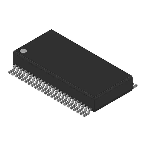
48-pin 300-mil SSOP Package (RoHS-Compliant)
Logic Block Diagram
A
5
A
6
A
7
A
8
A
9
A
11
A
12
A
13
A
14
DQ
0
DQ
1
DQ
2
DQ
3
DQ
4
DQ
5
DQ
6
DQ
7
Cypress Semiconductor Corporation
Document Number: 001-52040 Rev. *A
32K x 8 AutoStore™ nvSRAM with
Description
The Cypress STK17T88 combines a 256 Kb nonvolatile static
RAM (nvSRAM) with a full-featured real-time clock in a reliable,
monolithic integrated circuit.
The 256 Kb nvSRAM is a fast static RAM with a nonvolatile
Quantum Trap storage element included with each memory cell.
The SRAM provides the fast access and cycle times, ease of use
and unlimited read and write endurance of a normal SRAM. Data
transfers automatically to the nonvolatile storage cells when
power loss is detected (the STORE operation). On power up,
data is automatically restored to the SRAM (the RECALL
operation). Both STORE and RECALL operations are also
available under software control.
The real time clock function provides an accurate clock with leap
year tracking and a programmable, high accuracy oscillator. The
Alarm function is programmable for one-time alarms or periodic
minutes, hours, or days alarms. There is also a programmable
watchdog timer for processor control.
Quantum Trap
512 X 512
STORE
STATIC RAM
RECALL
ARRAY
512 X 512
COLUMN I/O
COLUMN DEC
A
A
A
A
A
A
0
1
2
3
4
10
•
198 Champion Court
Real Time Clock
V
V
CC
CAP
V
POWER
RTCbat
CONTROL
V
RTCcap
STORE/
RECALL
HSB
CONTROL
SOFTWARE
A
13
DETECT
RTC
A
MUX
14
,
•
San Jose
CA 95134-1709
Revised March 17, 2009
STK17T88
– A
0
X
1
X
2
INT
– A
0
G
E
W
• 408-943-2600
[+] Feedback
Advertisement
Table of Contents

Related Manuals for Cypress AutoStore STK17T88


Summary of Contents for Cypress AutoStore STK17T88
-
Page 1: Real Time Clock
Features ■ nvSRAM Combined With Integrated Real-Time Clock Functions (RTC, Watchdog Timer, Clock Alarm, Power Monitor) ■ Capacitor or Battery Backup for RTC ■ 25, 45 ns Read Access and R/W Cycle Time ■ Unlimited Read/Write Endurance ■ Automatic Nonvolatile STORE on Power Loss ■... -
Page 2: Pin Configurations
Pin Configurations Figure 1. 48-Pin SSOP (TOP) RTCbat Pin Descriptions Pin Name IO Type Input Address: The 15 address inputs select one of 32,768 bytes in the nvSRAM array or one of 16 bytes in the clock register map. Data: Bi-directional 8-bit data bus for accessing the nvSRAM and RTC. Input Chip Enable: The active low E input selects the device. -
Page 3: Absolute Maximum Ratings
Absolute Maximum Ratings Voltage on Input Relative to Ground...–0.5V to 4.1V Voltage on Input Relative to V ...–0.5V to (V Voltage on DQ or HSB ...–0.5V to (V Temperature under Bias ... –55°C to 125°C Junction Temperature ... –55°C to 140°C Storage Temperature ... -
Page 4: Ac Test Conditions
DC Characteristics (continued) = 2.7V-3.6V) Commercial Symbol Parameter Output Logic “1” Voltage Output Logic “0” Voltage Operating Temper- ature Operating Voltage Storage Capacitance Nonvolatile STORE operations DATA Data Retention AC Test Conditions Input Pulse Levels ...0V to 3V Input Rise and Fall Times ...≤ 5ns Input and Output Timing Reference Levels ... - Page 5 RTC DC Characteristics Symbol Parameter IBAK RTC Backup Current VRTCbat RTC Battery Pin Voltage VRTCcap RTC Capacitor Pin Voltage tOSCS RTC Oscillator time to start Document Number: 001-52040 Rev. *A Commercial Industrial Units — — — — — — Figure 4. RTC Component Configuration Recommended Values = 32.768 KHz = 10M Ohm...
- Page 6 SRAM READ Cycles #1 and #2 Symbols Alt. ELQV AVAV ELEH AVQV AVQV GLQV AXQX AXQX ELQX EHQZ GLQX GHQZ ELICCL EHICCH Figure 5. SRAM READ Cycle #1: Address Controlled ADDRESS DQ (DATA OUT) Figure 6. SRAM READ Cycle #2: E and G Controlled Notes 3.
- Page 7 SRAM WRITE Cycles #1 and #2 Symbols Alt. 12 t Write Cycle Time AVAV AVAV 13 t Write Pulse Width WLWH WLEH 14 t Chip Enable to End of Write ELWH ELEH 15 t Data Set-up to End of Write DVWH DVEH 16 t...
- Page 8 AutoStore/Power Up RECALL Symbols Standard Alternate Power up RECALL Duration HRECALL STORE Cycle Duration STORE HLHZ Low Voltage Trigger Level SWITCH CCRISE NOTE Read and Write cycles will be ignored during STORE, RECALL and while V Notes 9. t starts from the time V rises above V HRECALL 10.
- Page 9 Software-Controlled STORE/RECALL Cycle In the following table, the software controlled STORE and RECALL cycle parameters are listed. Symbols E Cont Alternate 26 t STORE / RECALL Initiation Cycle Time AVAV 27 t Address Set-up Time AVEL 28 t Clock Pulse Width ELEH 29 t Address Hold Time...
- Page 10 Hardware STORE Cycle Symbols Standard Alternate Hardware STORE to SRAM Disabled DELAY HLQZ Hardware STORE Pulse Width HLHX Soft Sequence Commands Symbols Standard Soft Sequence Processing Time Notes 14. On a hardware STORE initiation, SRAM operation continues to be enabled for time tDELAY to allow read/write cycles to complete 15.
-
Page 11: Mode Selection
MODE Selection 0x0E38 0x31C7 0x03E0 0x3C1F 0x303F 0x0FC0 0x0E38 0x31C7 0x03E0 0x3C1F 0x303F 0x0C63 Notes 17. The six consecutive addresses must be in the order listed. W must be high during all six consecutive cycles to enable a nonvolatile cycle. 18. - Page 12 nvSRAM Operation The STK17T88 nvSRAM is made up of two functional compo- nents paired in the same physical cell. These are the SRAM memory cell and a nonvolatile QuantumTrap™ cell. The SRAM memory cell operates like a standard fast static RAM. Data in the SRAM can be transferred to the nonvolatile cell (the STORE operation), or from the nonvolatile cell to SRAM (the RECALL operation).
- Page 13 Software STORE Data can be transferred from the SRAM to the nonvolatile memory by a software address sequence. The STK17T88 software STORE cycle is initiated by executing sequential E controlled READ cycles from six specific address locations in exact order. During the STORE cycle, previous data is erased and then the new data is programmed into the nonvolatile elements.
-
Page 14: Real Time Clock
Real Time Clock The clock registers maintain time up to 9,999 years in one-second increments. The user can set the time to any calendar time and the clock automatically keeps track of days of the week and month, leap years, and century transitions. There are eight registers dedicated to the clock functions which are used to set time with a write cycle and to read time during a read cycle. - Page 15 minute, have one second either shortened by 128 or lengthened by 256 oscillator cycles. If a binary “1” is loaded into the register, only the first 2 minutes of the 64 minute cycle is modified; if a binary 6 is loaded, the first 12 are affected, and so on.
- Page 16 Figure 15 is a functional diagram of the interrupt logic. Figure 15. Interrupt Block Diagram Watchdog Timer Power Monitor Driver VINT Clock Alarm Interrupt Register Watchdog Interrupt Enable (WIE). When set to 1, the watchdog timer drives the INT pin when a watchdog time-out occurs. When WIE is set to 0, the watchdog time-out only sets the WDF flag bit.
-
Page 17: Rtc Register Map
RTC Register Map Register 0x7FFF 10s Years 0x7FFE 0x7FFD 10s Day of Month 0x7FFC 0x7FFB 0x7FFA 10s Minutes 0x7FF9 10s Seconds 0x7FF8 OSCEN 0x7FF7 0x7FF6 WIE[0] AIE[0] PFE[0] 0x7FF5 0x7FF4 0x7FF3 10 Alarm Minutes 0x7FF2 10 Alarm Seconds 0x7FF1 10s Centuries 0x7FF0 *A binary value, not a BCD value. - Page 18 Register Map Detail 0x7FFF Contains the lower two BCD digits of the year. Lower nibble contains the value for years; upper nibble contains the value for 10s of years. Each nibble operates from 0 to 9. The range for the register is 0-99. 0x7FFE Contains the BCD digits of the month.
- Page 19 Register Map Detail (continued) Watchdog Write Enable. Set this bit to 1 to disable writing of the watchdog time-out value (WDT5-WDT0). This allows the user to strobe the watchdog without disturbing the time-out value. Setting this bit to 0 allows bits 5-0 to be written.
-
Page 20: Ordering Codes
Register Map Detail (continued) 0x7FF0 Watchdog Timer Flag. This read-only bit is set to 1 when the watchdog timer is allowed to reach 0 without being reset by the user. It is cleared to 0 when the Flags register is read or on power up Alarm Flag. -
Page 21: Package Diagram
STK17T88 Package Diagram Figure 16. 48-Pin SSOP (51-85061) 51-85061-*C Document Number: 001-52040 Rev. *A Page 21 of 22 [+] Feedback... - Page 22 Document History Page Document Title: STK17T88 32K x 8 AutoStore™ nvSRAM with Real-Time Clock Document Number: 001- 52040 ECN No. 2668660 GVCH/PYRS 2675319 Sales, Solutions, and Legal Information Worldwide Sales and Design Support Cypress maintains a worldwide network of offices, solution centers, manufacturer’s representatives, and distributors. To find the office closest to you, visit us at cypress.com/sales.
Need help?
Do you have a question about the AutoStore STK17T88 and is the answer not in the manual?
Questions and answers