
Related Manuals for Cypress T240HD


Summary of Contents for Cypress T240HD
- Page 1 CYW9P62S1-43012EVB-01 PSoC 62S1 Wi-Fi BT Pioneer Kit Guide Doc. # 002-28722 Rev. *B Cypress Semiconductor 198 Champion Court San Jose, CA 95134-1709 www.cypress.com Arrow.com. Downloaded from...
- Page 2 High-Risk Device, or to affect its safety or effectiveness. Cypress is not liable, in whole or in part, and you shall and hereby do release Cypress from any claim, damage, or other liability arising from any use of a Cypress product as a Critical Component in a High-Risk Device.
-
Page 3: Table Of Contents
3.2.6 I/O Headers....................37 3.2.7 CapSense Circuit ...................38 3.2.8 LEDs ......................39 3.2.9 Push Buttons....................40 3.2.10 Cypress Quad SPI NOR Flash...............40 3.2.11 Cypress Quad SPI F-RAM ................41 3.2.12 PSoC 6 USB ....................41 PSoC 62S1 Wi-Fi BT Pioneer Kit Rework ..............42 3.3.1 U.FL (UMCC) Connector for External Antenna ..........42 3.3.2 U.FL (UMCC) Connector for Antenna Diversity..........42... -
Page 4: Safety And Regulatory Compliance Information
This kit is not a finished product and when assembled may not be resold or otherwise marketed unless all required authorizations are first obtained. Contact support@cypress.com for details. The CYW9P62S1-43012EVB-01, as shipped from the factory, has been verified to meet with the requirements of CE as a Class A product. - Page 5 General Safety Instructions ESD Protection ESD can damage boards and associated components. Cypress recommends that you perform procedures only at an ESD workstation. If an ESD workstation is unavailable, use appropriate ESD protection by wearing an anti-static wrist strap attached to a grounded metal object.
-
Page 6: Introduction
You can use ModusToolbox™ to develop and debug your PSoC 6 MCU projects. ModusToolbox software is a set of tools that enable you to integrate Cypress devices into your existing development methodology. If you are new to PSoC 6 MCU and ModusToolbox IDE, refer to the application note... -
Page 7: Kit Contents
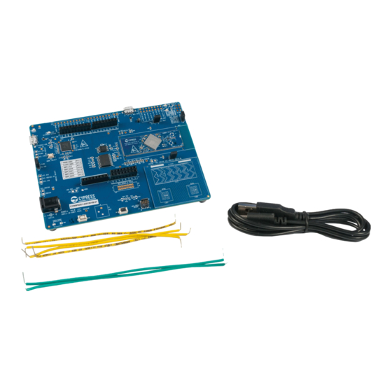
Quick Start Guide ■ Figure 1-1. Kit Contents Inspect the contents of the kit; if you find any part missing, contact your nearest Cypress sales office for help: www.cypress.com/support. CYW9P62S1-43012EVB-01 PSoC 62S1 Wi-Fi BT Pioneer Kit Guide, Doc. # 002-28722 Rev. *B Arrow.com. -
Page 8: Getting Started
These examples help you familiarize yourself with the PSoC 6 MCU and create your own design. These examples are available in various development ecosystems such as ModusToolbox IDE and Mbed OS. Visit Cypress’ code example page to access examples for the following development ecosystems: ModusToolbox based examples ❐... -
Page 9: Additional Learning Resources
Introduction Additional Learning Resources Cypress provides a wealth of data at www.cypress.com/psoc6 to help you to select the right PSoC device for your design and to help you to quickly and effectively integrate the device into your design. Technical Support... - Page 10 Introduction Table 1-2. Acronyms Used in this Document (continued) Acronym Definition Direct Memory Access External Crystal Oscillator Electrostatic Discharge GPIO General-Purpose Input/Output Human Interface Device Inter-Integrated Circuit Inter-IC Sound Integrated Circuit Integrated Development Environment Internet of Things Light-emitting Diode Low Power Oscillator Medium Access Control Out-of Box Personal Computer...
-
Page 11: Kit Operation
Kit Operation This chapter introduces you to various features of the PSoC 62S1 Wi-Fi BT Pioneer Board, including the theory of operation and the onboard KitProg3 programming and debugging functionality, USB-UART and USB-I2C bridges. Board Details The PSoC 62S1 Wi-Fi BT Pioneer Board is built around a PSoC 6 MCU. Figure 2-1 shows the block diagram of the PSoC 6 MCU device used on the board. - Page 12 Figure 2-2 shows the block diagram of the CYW9-BASE-01 Pioneer Board (modified for CYW9P62S1-43012EVB-01). Figure 2-3 shows the block diagram of the CYW9P62S1-43012CAR-01 Carrier Module. Figure 2-2. Block Diagram of Pioneer Board CYW9‐BASE‐01 Architecture Block Diagram Cypress Device 20‐pin ETM KitProg3 Mode 10‐pin SWD/ Reset Switch & LED JTAG Header...
- Page 13 Kit Operation Figure 2-4 shows the pinout of the PSoC 62S1 Wi-Fi BT Pioneer Board. Figure 2-4. PSoC 62S1 Wi-Fi BT Pioneer Board Pinout P1_0/SCL P1_1/SDA VREF/AREF GND/GND P0_4/D13 P0_3/D12 P0_2/D11 P0_5/D10 NC/D9 NC/D8 P1_4 VTARG/IOREF XRES/RESET 3.3/3.3V 5.0/5V GND/GND GND/GND VIN/Vin P10_0/A0...
- Page 14 Kit Operation Table 2-1. PSoC 62S1 Wi-Fi BT Pioneer Board Pinout (continued) Primary On-board Secondary On-board Connection details Function Function Orange user LED GPIO on non-Arduino P1[5] – (LED8) header IO7 (J24.2) P5[0] UART_RX Arduino D0 (J4.1) Remove R21 to disconnect from KitProg3. P5[1] UART_TX Arduino D1 (J4.2)
- Page 15 Kit Operation Table 2-1. PSoC 62S1 Wi-Fi BT Pioneer Board Pinout (continued) Primary On-board Secondary On-board Connection details Function Function Remove R24 to disconnect from CapSense. CapSense Button0 GPIO on non-Arduino P9[7] Populate R144 to connect to GPIO on non- header IO8 (J21.1) Arduino header.
- Page 16 Kit Operation The CYW9P62S1-43012EVB-01 PSoC 62S1 Wi-Fi BT Pioneer Kit comes with the PSoC 62S1 Wi-Fi BT Pioneer Board. Figure 2-5 Figure 2-6 show the markup of the Pioneer Board. Figure 2-5. PSoC 62S1 Wi-Fi BT Pioneer Board - Top View 29 14 13 14 CYW9P62S1-43012EVB-01 PSoC 62S1 Wi-Fi BT Pioneer Kit Guide, Doc.
- Page 17 Kit Operation Figure 2-6. PSoC 62S1 Wi-Fi BT Pioneer Board - Bottom View The PSoC 62S1 Wi-Fi BT Pioneer Board has the following components: 1. Power LED (LED1): This Yellow LED indicates the status of power supplied to board. 2. KitProg3 USB connector (J6): The USB cable provided along with the PSoC 62S1 Wi-Fi BT Pioneer Board connects between this USB connector and the PC to use the KitProg3 onboard programmer and debugger and to provide power to the board.
- Page 18 CYW43012 VDDIO power domain. 18. Cypress serial NOR flash memory (S25FS512S, U3): A S25FS512S NOR flash of 512-Mbit capacity is connected to the Quad SPI interface of the PSoC 6 MCU. The NOR device can be used for both data and code memory with execute-in-place (XIP) support and encryption.
- Page 19 Kit Operation 22. Cypress Quad SPI Ferroelectric-RAM (CY15V104QSN, U4): The CY15V104QSN is a 4-Mbit nonvolatile memory employing an advanced ferroelectric process. F-RAM is nonvolatile and per- forms reads and writes similar to a RAM. It provides reliable data retention for 151 years and is connected to the Quad SPI interface of the PSoC 6 MCU.
-
Page 20: Kitprog3: On-Board Programmer/Debugger
The PSoC 62S1 Wi-Fi BT Pioneer Board can be programmed and debugged using the onboard KitProg3. KitProg3 is an onboard programmer/debugger with additional USB-UART and USB-I2C functionality. A Cypress PSoC 5LP device is used to implement the KitProg3. For more details on the KitProg3 functionality, see the KitProg3 User Guide. - Page 21 Kit Operation b. Select the CYW9P62S1-43012EVB-01 in the Choose Board Support Package (BSP) window and click Next, as shown in Figure 2-9. Figure 2-9. New Application Creation: Choose Board Support Package (BSP) c. Select the application in the Choose Starter Application window and click Next, as shown in Figure 2-10.
- Page 22 Kit Operation 3. To build and program a PSoC 6 MCU application, in the Project Explorer, select <App_Name> project. In the Quick Panel, scroll to the Launches section and click the <App_Name> Program (KitProg3) configuration as shown in Figure 2-12. Figure 2-12.
- Page 23 Kit Operation 2.2.1.1 Using the OOB Example – PSoC 6 MCU: Hello World The PSoC 62S1 Wi-Fi BT Pioneer Board is by default programmed with the code example: PSoC 6 MCU: Hello World. The steps below describe how to use the example. For a detailed description of the project refer to the example’s readme file in the GitHub repository.
-
Page 24: Usb-Uart Bridge
Kit Operation 2.2.2 USB-UART Bridge The KitProg3 on the PSoC 62S1 Wi-Fi BT Pioneer Board can act as a USB-UART bridge. The KitProg 3 has two USB-UART bridges. The primary UART is connected to the PSoC 6 MCU and the secondary UART is connected to the CYW43012. The primary UART can always be accessed through USB, while the secondary UART can be accessed by changing the mode of the KitProg3 to BULK with two UARTs Mode. -
Page 25: Usb-I2C Bridge
Kit Operation 2.2.3 USB-I2C Bridge The KitProg3 can function as a USB-I2C bridge and can communicate with the Bridge Control Panel (BCP) software which acts as an I2C master. The I2C lines on the PSoC 6 MCU are hard-wired on the board to the I2C lines of the KitProg3, with onboard pull-up resistors as Figure 2-17 shows. -
Page 26: Hardware
Hardware Schematics Refer to the schematic files available in the webpage. Hardware Functional Description This section explains in detail the individual hardware blocks. 3.2.1 CYW9P62S1-43012CAR-01 (MOD1) CYW9P62S1-43012CAR-01 PSoC 6 (1M) with CYW43012 USI SiP Carrier Module is a castellated PCB module which consists mainly of an USI SiP module, WM-BAC-CYW-50, with a PSoC 6 MCU and CYW43012. - Page 27 Hardware Decoupling Capacitors VDDA VDDD VDDIO0 VBACKUP VDD_NS VDDUSB VBAT VDDIO_WL 10uF 10uF 10uF 10uF USI SiP Module PSoC 6 MCU Signals WCO_P0_0 P0_0 P7_0 P7_0 WCO_P0_1 P7_1 P0_1 P7_1 P7_2 P0_2 P0_2 P7_2 P7_7 P0_3 P0_3 P7_7 P0_4 P0_4 P0_5 P9_0 P0_5...
- Page 28 Hardware USI SiP Module CYW43012 Signals SDIO_DATA0 SDIO_DATA0 RF_OUT 8.2pF RF_SW_IN SDIO_DATA1 SDIO_DATA1 MAIN_ANT SDIO_DATA2 SDIO_DATA2 SDIO_DATA3 SDIO_DATA3 RF_SW_CTRL_4 SDIO_CMD SDIO_CMD RF_SW_CTRL_4 SDIO_CLK SDIO_CLK RF_SW_CTRL_5 VOUT_3P3 WL_UART_RX WL_JTAG_TDI WL_UART_TX WL_JTAG_TRS WL_REG_ON WL_REG_ON VOUT_3P3 WL_HOST_WAKE WL_HOST_WAKE BT_UART_TXD BT_UART_TXD BT_UART_RXD BT_UART_RXD BT_UART_CTS BT_UART_CTS_L BT_UART_RTS BT_UART_RTS_L...
- Page 29 Hardware Carrier Module Footprint (Power) VDDA MOD1A VBAT VDDA_MCU VBAT_WL VBAT_WL VDDD VDDIO_WL VDDD_MCU VDDIO_WL VDDIO0_MCU VCCD_MCU VDDIO0 VDDIO1_MCU VDDIO1 *Note VDDIO2_MCU VDD_NS VDD_NS_MCU VBACKUP GND_1 GND_2 VBACKUP_MCU GND_3 GND_4 VDDUSB GND_5 GND_6 VDDUSB_MCU GND_7 Carrier Module Footprint Note: In WM-BAC-CYW-50, VDDIO0 & VDDIO1 need to be same v oltage as VDDIO_WL. VDDIO2_MCU w ill be same v oltage as VDDIO_WL as per baseboard design, the reason VDDIO0 &...
- Page 30 Hardware Carrier Module Footprint (PSoC 6 MCU Signals) MOD1B 0 OHM P1_0 P1_5 I2C_SCL CSX_TX P1_1 I2C_SDA P9_7 CSB_0 P7_0 ARD_AREF CSB_1 P10_0 ARD_A0 CSS_0 P9_0 P10_1 ARD_A1 CSS_1 P9_1 0 OHM P6_4 P9_2 ARD_A2 CSS_2 0 OHM P6_5 P9_3 ARD_A3 CSS_3 P10_4...
-
Page 31: Psoc 5Lp-Based Kitprog3 (U2)
Hardware 3.2.2 PSoC 5LP-based KitProg3 (U2) An onboard PSoC 5LP (CY8C5868LTI-LP039) device is used as KitProg3 to program and debug PSoC 6 MCU. The PSoC 5LP device connects to the USB port of a PC through a USB connector and to the SWD and other communication interfaces of PSoC 6 MCU. The PSoC 5LP device is a true system-level solution providing MCU, memory, analog, and digital peripheral functions in a single chip. -
Page 32: Serial Interconnection Between Psoc 5Lp And Psoc 6 Mcu
Hardware 3.2.3 Serial Interconnection between PSoC 5LP and PSoC 6 MCU In addition to the use as an onboard programmer, the PSoC 5LP device functions as an interface for the USB-UART and USB-I2C bridges, as shown in Figure 3-3. The USB-Serial pins of the PSoC 5LP device are hard-wired to the I2C/UART pins of the PSoC 6 MCU. -
Page 33: Serial Interconnection Between Psoc 5Lp And Cyw43012
Hardware 3.2.4 Serial Interconnection Between PSoC 5LP and CYW43012 The PSoC 5LP device also has a secondary UART that is connected to the BT_UART of the CYW43012 (USI WM-BAC-CYW-50). Figure 3-4. Serial Interconnection Between PSoC 5LP and CYW43012 KitProg3 Secondary UART Multiplexing KitProg3 Level Translator for Secondary UART and GPIO 0 OHM B_UART_2_TX... - Page 34 Hardware 3.2.5.1 Voltage regulators The power supply system is designed for the voltage configurations listed in Table 3-1. Some configurations achievable on this kit are outside the operating range for the device. However, it is not possible to achieve all applicable configurations by changing jumper positions but rather requires re- work of respective 0-ohm resistors.
- Page 35 Hardware 3.2.5.2 Voltage Selection VCC_VBAT has a dedicated regulator that changes voltage by varying the feedback voltage through the resistor network at J9. VTARG and VCC_VDDIO2_IN have dedicated 3-pin voltage selection headers J14 and J16 respectively that select between VCC_3V3 or VCC_1V8 voltages. Figure 3-7 shows the schematics of the power selection circuits.
- Page 36 Hardware 3.2.5.3 Current Measurement Headers The current of the following domains have dedicated 2-pin headers to facilitate easy current mea- surement using an ammeter across the pins. Note: If Header is not loaded by default, it is by-passed by a 0-ohm resistor parallel to it. Please make sure to remove the corresponding 0-ohm resistor (as per Figure 3-9) before measuring current...
-
Page 37: I/O Headers
Hardware 3.2.6 I/O Headers 3.2.6.1 Arduino-compatible Headers (J1, J2, J3, J4) The board has four Arduino-compatible headers: J1, J2, J3, and J4. You can connect 3.3 V Arduino- compatible shields to develop applications based on the shield’s hardware. Note: 5-V shields are not supported and connecting a 5-V shield may permanently damage the board. -
Page 38: Capsense Circuit
Hardware 3.2.7 CapSense Circuit A CapSense slider and two buttons, all supporting both self-capacitance (CSD) and mutual- capacitance (CSX) sensing are connected to PSoC 6 MCU as Figure 3-11 shows. Three external capacitors - CMOD for CSD, CINTA and CINTB for CSX - are present on the CYW9P62S1- 43012CAR-01. -
Page 39: Leds
Hardware 3.2.8 LEDs LED2 (Yellow) indicates the status of KitProg3 (See the KitProg3 User Guide for details). LED1 (Yellow) indicates the status of the power supplied to the board. The board also has two user-controllable LEDs (LED8 and LED9) connected to PSoC 6 MCU pins for user applications. -
Page 40: Push Buttons
3.2.10 Cypress Quad SPI NOR Flash The PSoC 62S1 Wi-Fi BT Pioneer Board has a Cypress NOR flash memory (S25FS512SAGM- FI010) of 512Mb capacity. The NOR flash is connected to the Quad SPI interface of the PSoC 6 MCU device. The NOR flash device can be used for both data and code with execute-in-place (XIP) support and encryption. -
Page 41: Cypress Quad Spi F-Ram
Hardware 3.2.11 Cypress Quad SPI F-RAM The PSoC 62S1 Wi-Fi BT Pioneer Board contains the CY15V104QSN Excelon™ F-RAM device, which can be accessed through Quad SPI interface. The F-RAM is 4-Mbit (512K × 8) and is capable of Quad SPI speed up to 108 MHz but on this kit it is limited to 75 MHz. -
Page 42: Psoc 62S1 Wi-Fi Bt Pioneer Kit Rework
Hardware PSoC 62S1 Wi-Fi BT Pioneer Kit Rework 3.3.1 U.FL (UMCC) Connector for External Antenna The RF output of CYW43012 is connected to the chip antenna by default. To disconnect the chip antenna and connect an external antenna, remove C13 and populate C11, J1 on CYW9P62S1- 43012CAR-01. -
Page 43: Frequently Asked Questions
Hardware Frequently Asked Questions 1. How does CYW9P62S1-43012EVB-01 handle a voltage connection when multiple power sources are plugged in? There are three different options to power the baseboard; KitProg3 Micro-B USB connector (J6), PSoC 6 Micro-B USB connector (J7), and External DC supply via VIN connector (J5). The voltage from each of the sources in passed through ORing diodes that supply VCC_IN. -
Page 44: Revision History
Revision History Document Revision History Document Title: CYW9P62S1-43012EVB-01 PSoC 62S1 Wi-Fi BT Pioneer Kit Guide Document Number: 002-28722 Revision Issue Date Description of Change Number 6707976 12/17/2019 New kit guide. 6768042 01/07/2020 Updated Hardware chapter on page Updated “Hardware Functional Description” on page Updated “CYW9P62S1-43012CAR-01 (MOD1)”...
Need help?
Do you have a question about the T240HD and is the answer not in the manual?
Questions and answers