Sign In
Upload
Manuals
Brands
IEI Technology Manuals
Single board computers
WAFER-MARK
IEI Technology WAFER-MARK Manuals
Manuals and User Guides for IEI Technology WAFER-MARK. We have
1
IEI Technology WAFER-MARK manual available for free PDF download: User Manual
IEI Technology WAFER-MARK User Manual (195 pages)
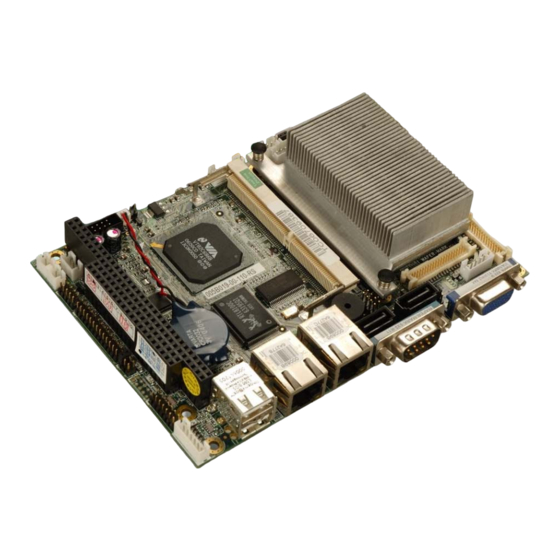
3.5" SBC with VIA MARK 533MHz/800MHz CPU on-board with SATA, Audio, VGA/LVDS/ TTL and Dual LAN
Brand:
IEI Technology
| Category:
Single board computers
| Size: 5.36 MB
Table of Contents
Table of Contents
7
1 Introduction
21
Figure 1-1: WAFER-MARK Embedded SBC
22
Table 1-1: WAFER-MARK Board Variations
22
Figure 1-2: WAFER-MARK Overview
24
Wafer-Mark Overview
24
Figure 1-3: WAFER-MARK Solder Side Overview
25
Technical Specifications
26
Table 1-2: Technical Specifications
28
WAFER-MARK Connectors
25
Wafer-Mark Overview
22
WAFER-MARK Board Variations
22
WAFER-MARK Applications
23
WAFER-MARK Benefits
23
WAFER-MARK Features
23
2 Detailed Specifications
29
Dimensions
30
Board Dimensions
30
External Interface Panel Dimensions
30
Figure 2-1: WAFER-MARK Dimensions (MM)
30
Overview
30
Data Flow
31
Figure 2-3: Data Flow Block Diagram
31
Table 2-1: Supported HDD Specifications
34
VIA VT82C686B Audio Codec 97 (AC'97) Controller
35
VIA VT82C686B Infrared Interface
36
VIA VT82C686B Parallel Port Communications
36
VIA VT82C686B Serial Communications
36
VIA VT82C686B USB Controller
36
Bios
37
VIA VT82C686B Keyboard and Mouse
37
VIA VT82C686B Real Time Clock
37
Pci Bus
38
10/100M Ethernet
38
Overview
38
SATA Drive Controller
39
Environmental and Power Specifications
39
Operating Temperature and Temperature Control
39
System Monitoring
39
Power Consumption
40
Figure 2-2: External Interface Panel Dimensions (MM)
31
Cpu Support
32
VIA MARK Overview
32
VIA MARK Memory Support
32
VIA MARK Integration
32
VIA MARK S3 Graphics Prosavage4 Graphics Core
33
VIA MARK VIA Padlock Security Engine
33
System Chipset
33
VIA VT82C686B ATA-6 Controller
34
VIA VT82C686B Flash Interface
34
Table 2-2: Power Consumption
40
3 Unpacking
41
Anti-Static Precautions
42
Unpacking
42
Unpacking Precautions
42
Unpacking Checklist
43
Package Contents
43
Optional Components
44
Table 3-1: Package List Contents
44
Table 3-2: Optional Components
44
4 Connector Pinouts
45
Figure 4-1: Connector and Jumper Locations
46
Table 4-3: at Power Connector Pinouts
50
Figure 4-3: at Power Connector Location
50
Figure 4-4: ATX Power Supply Enable Connector Location
51
Table 4-4: ATX Power Supply Enable Connector Pinouts
51
Audio CD in Connector
52
Figure 4-5: Audio Connector Pinouts (10-Pin)
52
Table 4-5: Audio Connector Pinouts (10-Pin)
52
Backlight Inverter Connector
53
Figure 4-6: Audio CD in Connector Pinouts (4-Pin)
53
Table 4-6: Audio CD in Connector Pinouts
53
Battery Connector
54
Table 4-7: Panel Backlight Connector Pinouts
54
Compact Flash Socket
55
Audio Connector
51
Peripheral Interface Connectors
46
WAFER-MARK Layout
46
Figure 4-2: Connector and Jumper Locations (Solder Side)
47
Table 4-1: Peripheral Interface Connectors
48
Table 4-2: Rear Panel Connectors
49
ATX Power Supply Enable Connector
50
Internal Peripheral Connectors
49
AT Power Connector
49
Peripheral Interface Connectors
47
External Interface Panel Connectors
48
Figure 4-7: Panel Backlight Connector Pinout Locations
54
Table 4-10: +5V Fan Connector Pinouts
58
Figure 4-11: 26-Pin FDD Connector Location
59
Figure 4-12: GPIO Connector Pinout Locations
60
GPIO Connector
60
Table 4-11: 26-Pin FDD Connector Pinouts
60
Table 4-12: GPIO Connector Pinouts
60
Figure 4-13: Secondary IDE Device Connector Locations
62
Figure 4-14: Infrared Connector Pinout Locations
63
Infrared Interface Connector
63
Table 4-13: Secondary IDE Connector Pinouts
63
Figure 4-15: Keyboard/Mouse Connector Location
64
Keyboard/Mouse Connector
64
Table 4-14: Infrared Connector Pinouts
64
Figure 4-16: LED Connector Locations
65
LED Connector
65
Table 4-15: Keyboard/Mouse Connector Pinouts
65
Figure 4-17: Parallel Port Connector Location
66
Parallel Port Connector
66
Table 4-16: LED Connector Pinouts
66
PC/104 Slot
67
Table 4-17: Parallel Port Connector Pinouts
67
Figure 4-18: PC/104 Slot Location
68
Figure 4-19: PC/104 Power Input Connector Pinouts
70
PC/104 Power Input Connector
70
Table 4-18: PC/104 Slot Connector Pinouts
70
Figure 4-20: Power Button Connector Location
71
Power Button Connector
71
Reset Button Connector
71
Table 4-19: PC/104 Power Input Connector Pinouts
71
Table 4-20: Power Button Connector Pinouts
71
Figure 4-21: Reset Button Connector Locations
72
SATA Drive Connectors
72
Table 4-21: Reset Button Connector Pinouts
72
Figure 4-22: SATA Drive Connector Locations
73
Serial Port Connector (RS-422/485)
73
Table 4-22: SATA Drive Connector Pinouts
73
Figure 4-23: Serial Port Connector Pinout Locations
74
Table 4-23: Serial Port Connector Pinouts
74
TFT LCD LVDS Connector
74
Figure 4-24: TFT LCD LVDS Connector Pinout Locations
75
Table 4-24: TFT LCD LVDS Port Connector Pinouts
76
TFT LCD TTL Connector
76
Figure 4-25: TFT LCD TTL Connector Pinout Locations
77
Figure 4-26: USB Connector Pinout Locations
78
Table 4-25: TFT LCD TTL Port Connector Pinouts
78
USB Connector (Internal)
78
Ethernet Connector
79
External Peripheral Interface Connector Overview
79
External Peripheral Interface Connectors
79
Figure 4-27: WAFER-MARK On-Board External Interface Connectors
79
Table 4-26: USB Port Connector Pinouts
79
Figure 4-28: J7 Connector
80
Keyboard/Mouse Connector (Optional)
80
Table 4-27: RJ-45 Ethernet Connector Pinouts
80
Table 4-28: LAN Connector Leds
80
Figure 4-29: PS/2 Pinout and Configuration
81
Serial Port Connector (COM 1)
81
Table 4-29: Keyboard Connector Pinouts
81
Figure 4-30: COM1 Pinout Locations
82
Table 4-30: RS-232 Serial Port (COM 1) Pinouts
82
USB Combo Port
82
VGA Connector
83
Figure 4-8: Battery Connector Location
55
Table 4-8: Battery Connector Pinouts
55
Table 4-9: CF Card Socket Pinouts
57
Figure 4-10: +5V Fan Connector Location
58
Floppy Disk Connector (Optional)
58
IDE Connector
61
Figure 4-9: CF Card Socket Location
56
Fan Connector
57
Figure 4-31: VGA Connector
83
Table 4-31: USB Connector Pinouts
83
Table 4-32: VGA Connector Pinouts
83
5 Installation
85
Anti-Static Precautions
86
Installation Considerations
87
Installation Notices
87
Installation Checklist
88
Figure 5-1: SO-DIMM Installation
89
Figure 5-2: CF Card Installation
91
Table 5-1: Jumpers
92
COM 2 Function Select Jumper
93
Clear CMOS Jumper
92
So-DIMM Installation and Cf Card Installation
89
SO-DIMM Installation
89
CF Card Installation
90
Jumper Settings
91
Table 5-2: Clear CMOS Jumper Settings
93
Figure 5-3: Clear CMOS Jumper
93
Figure 5-4: COM 2 Function Select Jumper Location
94
Table 5-3: COM 2 Function Select Jumper Settings
94
COM 1/2 Pin 9 Setting Jumper (Optional)
95
Table 5-4: LCD Voltage Selection Jumper Settings
95
Figure 5-6: COM 1/2 Pin 9 Setting Jumper Location
96
Table 5-6: IEI Provided Cables
98
ATA Flat Cable Connection
99
ATX Power Connection
100
LCD Voltage Selection
94
Figure 5-5: LCD Voltage Selection Jumper Location
95
Figure 5-7: Audio Kit Cable Connection
98
Figure 5-10: Connect ATX Power Adapter Cable to Power Supply
101
Figure 5-11: Connect ATX Power Cable to Motherboard
102
Figure 5-12: Dual RS-232 Cable Installation
103
Keyboard/Mouse Y-Cable Connector
103
Figure 5-13: Keyboard/Mouse Y-Cable Connection
104
SATA Drive Connection
104
Figure 5-14: SATA Drive Cable Connection
105
External Peripheral Interface Connection
106
Figure 5-15: SATA Power Drive Connection
106
LAN Connection
106
Figure 5-16: LAN Connection
107
Serial Device Connection
107
USB Connection
108
Figure 5-8: IDE Cable Connection
100
Figure 5-9: Power Cable to Motherboard Connection
101
Dual RS-232 Cable Connection
102
Table 5-5: COM 1/2 Pin 9 Setting Jumper Settings
96
Chassis Installation
97
Airflow
97
Motherboard Installation
97
Internal Peripheral Device Connections
97
Peripheral Device Cables
97
Audio Kit Installation
98
Figure 5-17: Serial Device Connector
108
Figure 5-18: USB Connector
109
6 Award Bios
111
Introduction
112
Starting Setup
112
Using Setup
112
Getting Help
113
Unable to Reboot after Configuration Changes
113
Main BIOS Menu
113
Table 6-1: BIOS Navigation Keys
113
BIOS Menu 1: Award BIOS CMOS Setup Utility
114
Standard Cmos Features
116
BIOS Menu 2: Standard CMOS Features
116
IDE Primary Master/Slave
117
Advanced Bios Features
120
BIOS Menu 3: Advanced BIOS Features
120
Advanced Chipset Features
122
BIOS Menu 4: Advanced Chipset Features
123
Integrated Peripherals
124
BIOS Menu 5: Integrated Peripherals
125
Power Management Setup
129
BIOS Menu 6: Power Management Setup
129
Wake up Events
130
BIOS Menu 7: Wake up Events
131
Pnp/Pci Configurations
132
BIOS Menu 8: Pnp/Pci Configurations
133
Pc Health Status
135
BIOS Menu 9: PC Health Status
135
7 Software Drivers
137
Available Software Drivers
138
Via 4 in 1 Chipset Driver Installation
138
Figure 7-3: VIA Chipset Driver Installation Welcome Screen
139
Figure 7-2: Setup Utility Icon
139
Figure 7-1: Access the 4In1_Extreme Folder
139
Figure 7-4: Readme Information
140
Figure 7-5: VIA Chipset Driver Installation Type
141
Figure 7-6: Driver Selection
142
Figure 7-7: VIA PCI IDE Bus Driver Selection
143
Figure 7-8: AGP Driver Selection
144
Figure 7-9: Restart the Computer
145
Figure 7-10: Access the Audio Driver Folder
145
Realtek Audio Driver Installation
145
Figure 7-12: Audio Driver Install Shield Wizard Starting
146
Figure 7-11: Setup Utility Icon
146
Figure 7-13: Audio Driver Setup Preparation
147
Figure 7-14: Audio Driver Welcome Screen
148
Figure 7-15: Audio Driver Software Configuration
148
Figure 7-16: Audio Driver Digital Signal
149
Figure 7-17: Audio Driver Installation Begins
150
LAN Driver Installation
151
Figure 7-18: Audio Driver Installation Complete
151
Figure 7-19: Access the LAN Driver Folder
151
Figure 7-20: Setup Utility Icon
152
Figure 7-21: LAN Driver Welcome Screen
152
Figure 7-22: LAN Driver Installation Complete
153
Abios Options
155
Bgpio Connection
159
Dio Interface Introduction
160
Dio Connector Pinouts
160
Assembly Language Samples
161
Enable the DIO Input Function
161
Enable the DIO Output Function
161
Cwatchdog Timer
163
Daddress Mapping
167
Address Map
168
St Mb Memory Address Map
168
Irq Mapping Table
169
Dma Channel Assignments
169
Eexternal Ac'97 Audio Codec
171
Introduction
172
Accessing the AC'97 CODEC
172
Driver Installation
172
Sound Effect Configuration
173
Accessing the Sound Effects Manager
173
Sound Effect Manager Configuration Options
174
Fraid Setup
177
Introduction
178
Precautions
178
Features and Benefits
179
Accessing the al Iraid Utility
179
Raid Options
181
Create RAID 0 Striping for Performance
181
Create RAID 1 Mirroring for Reliability
183
Create JBOD for Integrated Capacity
185
Stripe Size
186
Delete RAID Setting & Partition
187
Delete All RAID Setting & Partition
187
Rebuild RAID Array
188
Select Boot Drive
188
Gindex
189
Advertisement
Advertisement
Related Products
IEI Technology WAFER-ULT-i1
IEI Technology WAFER-ULT2-i1
IEI Technology WAFER-945GSE3
IEI Technology WAFER-CV-N25501 Series
IEI Technology WAFER-EHL-J6412
IEI Technology WAFER-JL-N5105
IEI Technology WAFER-JL-N5105-R10
IEI Technology WAFER-945GSE-N270
IEI Technology WAFER-ATOM
IEI Technology WAFER-9371A
IEI Technology Categories
Motherboard
Touch Panel
Computer Hardware
Single board computers
Desktop
More IEI Technology Manuals
Login
Sign In
OR
Sign in with Facebook
Sign in with Google
Upload manual
Upload from disk
Upload from URL