
Related Manuals for Cypress CY3663


Summary of Contents for Cypress CY3663
- Page 1 CY3663 Hardware User’s Manual Version 1.5 Cypress Semiconductor 3901 North First Street San Jose, CA 95134 Tel.: (800) 858-1810 (toll-free in the U.S.) (408) 943-2600 www.cypress.com www.DataSheet.in...
- Page 2 Company’s stan- CY16 is a trademark of the Cypress Corpora- dard warranty which is detailed in Cypress’s tion. All other product names are trademarks Terms and Conditions located on the Com- are registered trademarks of their respective pany’s web site.
-
Page 3: Table Of Contents
Table of Contents Chapter 1. Introduction 1.1 Introduction........................1-1 Chapter 2. Cypress StrongARM Single Board Computer 2.1 Introduction........................2-1 2.2 System Block Diagram ....................2-2 2.3 Processor and Memory ....................2-3 2.4 Serial Ports........................2-3 2.4.1 Serial Port #1....................2-3 2.4.2 Serial Port #2.................... - Page 4 3.8.4 Pushbuttons..................... 3-7 3.9 Power ........................... 3-7 3.10 USB Ports ........................3-7 3.11 Miscellaneous......................3-8 Chapter 4. Cypress EZ-OTG Development Board 4.1 Introduction ........................4-1 4.2 System Block Diagram ....................4-1 4.3 Processor and Memory ....................4-2 4.4 Asynchronous Serial Ports ................... 4-3 4.4.1 UART.......................
- Page 5 (Table of Contents) Chapter 5. Developing with the EZ-Host and EZ-OTG Boards 5.1 Standalone Mode Operation ..................5-1 5.1.1 Power-up EEPROM Selection................. 5-1 5.1.2 DIP Switches ....................5-1 5.1.3 Pushbutton Inputs.................... 5-1 5.1.4 LEDs: OTG ERROR, SESSION ACTIVE, HOST, PERIPHERAL ....5-1 5.1.5 LEDs: RUN/STOP ...................
- Page 6 6.1 Normal Operation of the Cypress StrongARM SBC............. 6-1 6.1.1 Running Design Examples ................6-1 6.1.2 Operation as a Linux USB Muti-port Host ............6-1 6.2 Linux Development with the Cypress StrongARM SBC ..........6-2 6.2.1 Boot Sequence ....................6-2 6.2.2 Using Ethernet Downloads During Development ..........6-3 6.2.2.1 Updating FLASH contents over Ethernet ..........
- Page 7 User Interface ....................2-7 Figure 3-1. Cypress EZ-Host Development Board .............. 3-1 Figure 3-2. Cypress EZ-Host Development Board - Block Diagram ........3-3 Figure 3-3. EZ-Host User Interface ..................3-5 Figure 4-1. Cypress EZ-OTG Development Board - Block Diagram ........4-2 Figure 5-1.
- Page 8 List of Figures www.DataSheet.in...
-
Page 9: Chapter 1. Introduction
Chapter 1. Introduction Introduction This manual describes the hardware in the Cypress CY3663 Development Kit (DVK). The three individual boards included in the kit are the Cypress StrongARM Single Board Computer (SBC), the EZ-Host DVK board, and the EZ-OTG DVK board. The next three chapters provide a descrip- tion of the hardware circuitry on each of the boards, and the last two chapters give the developer details on using the boards. - Page 10 CY3663 Hardware User’s Guide Page 1-2 CY3663 Hardware User’s Guide v1.5 www.DataSheet.in...
-
Page 11: Chapter 2. Cypress Strongarm Single Board Computer
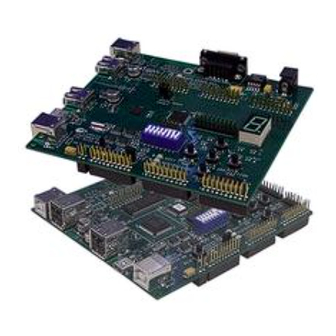
Chapter 2. Cypress StrongARM Single Board Computer Introduction Figure 2-1. Cypress StrongARM Single Board Computer The Cypress StrongARM Single Board Computer (SBC) is a versatile development platform that currently supports the Linux operation system. Other features include: • 133 MHz Intel StrongARM SA-1110 microprocessor •... -
Page 12: System Block Diagram
Multiple synchronous and asynchronous serial ports • High signal visibility with quick connect logic analyzer support • Robust buffered expansion port System Block Diagram The following is a block diagram of the Cypress StrongARM SBC. EEPROM CPLD Programming Programming 2 Line LCD... -
Page 13: Processor And Memory
Processor and Memory The Cypress StrongARM SBC uses the Intel StrongARM SA-1110 microprocessor running at 133 MHz. The SA-1110 has built-in serial ports, memory management unit, programmable chip select unit, interrupt controller, JTAG interface, instruction cache, data cache, and programmable mem- ory controller. -
Page 14: Serial Port #2
Buffered 16-bit or 32-bit data bus, buffered address bus, buffered bus control, and buff- ered master active low reset • Interrupt support • Direct connection to several GPIO pins on StrongARM SA-1110 • Direct connection to UART and synchronous serial port on SA-1110 Page 2-4 CY3663 Hardware User’s Guide v1.5 www.DataSheet.in... -
Page 15: Figure 2-4. Sbc Expansion Port Location
3.3 volt and 5 volt power from SBC. • Expansion port connectors in 20-pin dual row connectors, which are compatible with Agi- lent logic analyzer terminator adapters. Figure 2-4. SBC Expansion Port Location Chapter 2. Cypress StrongARM Single Board Computer Page 2-5 www.DataSheet.in... -
Page 16: Cpld
PCA flex and possible damage. CPLD The CPLD is a Cypress Delta39K series part offering high density, great flexibility, and easy in-sys- tem programming. The configuration for the CPLD is stored in U25, which is a serial EEPROM. At power-up, the CPLD loads the configuration from the EEPROM, then allows the board to come out of reset. -
Page 17: User Interface
D5 – Green LED lit when 5 volts is available • D7 – Green LED lit when 3.3 volts is available • D1 – Green LED lit when 1.55 volts is available (used for the SA-1110 core) Chapter 2. Cypress StrongARM Single Board Computer Page 2-7 www.DataSheet.in... -
Page 18: General Purpose Leds
The SBC receives power from a 5 volt regulated wall transformer. Power is fused on board by the fast acting non-resetable fuse at F1. 5 volts is distributed around the board and to the expansion Page 2-8 CY3663 Hardware User’s Guide v1.5 www.DataSheet.in... -
Page 19: Miscellaneous Jumpers
J44 – This header connects to an in-circuit EEPROM programmer for CPLD configuration updates. • Unloaded components and connections – There are several unloaded component and connector footprints on the PCB. These are for future use and have not been tested. Chapter 2. Cypress StrongARM Single Board Computer Page 2-9 www.DataSheet.in... - Page 20 CY3663 Hardware User’s Guide Page 2-10 CY3663 Hardware User’s Guide v1.5 www.DataSheet.in...
-
Page 21: Chapter 3. Cypress Ez-Host Development Board
Chapter 3. Cypress EZ-Host Development Board Introduction The Cypress EZ-Host development board is a versatile development platform used to demonstrate and develop with the Cypress EZ-Host USB host/peripheral controller (CY7C67300). Figure 3-1. Cypress EZ-Host Development Board Other features include: •... - Page 22 40-pin IDE connector • User selectable operation either in standalone mode or co-processor mode • Support for co-processor mode connection to the Cypress StrongARM SBC • Support for power from external wall transformer or co-processor Page 3-2 CY3663 Hardware User’s Guide v1.5...
-
Page 23: System Block Diagram
System Block Diagram The following is a block diagram of the Cypress EZ-Host development board containing the Cypress EZ-Host USB host/peripheral controller (CY7C67300). EEPROM GPIO 12 MHz EEPROM SRAM xcvr GPIO ADDRESS RS-232 EEPROM DIP switches - 8 CY7C67300 DATA... -
Page 24: Asynchronous Serial Ports
J25 and J30 (signal names GPIO_16, GPIO_17, GPIO_18, GPIO_26). If the EZ-Host board is connected as a co-processor to the Cypress StrongARM SBC and HSS operation is selected by the appropriate DIP switch settings, the HSS port communicates with one of the serial ports on the SBC. -
Page 25: Co-Processor Connection
The EZ-Host board has a group of connectors (J24, J25, J26, J29, J30, J31, J32) which allow con- nection of it to the Cypress StrongARM SBC. The DIP switches configure the EZ-Host board for operation in one of the three co-processor modes: HPI, SPI, or HSS. -
Page 26: Seven Segment Display
D6 – Green general purpose LED. Note: When in stand-alone mode, D1, D7, D8, and D9 are driven by the CY7C67300. When in co-processor mode, these four LEDs are driven by the Cypress StrongARM SBC. Page 3-6 CY3663 Hardware User’s Guide v1.5... -
Page 27: Ide Led
J23. Pushbuttons S1 through S5 are general purpose input but- tons that are used during the operation of the design examples. Note that the pushbuttons are read and cleared by the CY7C67300 in stand-alone mode and by the Cypress StrongARM SBC in co-processor mode. -
Page 28: Miscellaneous
R19, R21, and R22 are loaded and R47 and R49 are removed. • Debug headers – All the 20-pin headers on the board are compatible with Agilent logic analyzer terminator adapters. This feature allows quick and simple debug connection. Page 3-8 CY3663 Hardware User’s Guide v1.5 www.DataSheet.in... -
Page 29: Chapter 4. Cypress Ez-Otg Development Board
• Support for power from external wall transformer or co-processor System Block Diagram The following is a block diagram of the Cypress EZ-OTG development board containing the Cypress EZ-OTG USB host/peripheral controller (CY7C67200). Chapter 4. Cypress EZ-OTG Development Board Page 4-1... -
Page 30: Processor And Memory
Expansion Port Figure 4-1. Cypress EZ-OTG Development Board - Block Diagram Processor and Memory The Cypress EZ-OTG development board is centered around the Cypress EZ-OTG USB host/ peripheral controller (CY7C67200). This USB controller has several on-chip features as listed below: •... -
Page 31: Asynchronous Serial Ports
The EZ-OTG board has a group of connectors (J24, J25, J26, J29, J30, J31, J32) which allow con- nection of it to the Cypress StrongARM SBC. But even in standalone mode, the UART should not be used if the firmware accesses the DIP switches or SSD on the board. The DIP switches config- ure the EZ-OTG board for operation in one of the three co-processor modes: HPI, SPI, or HSS. -
Page 32: Cpld
CY3663 Hardware User’s Guide Note: Be careful when removing this board from the expansion port of the Cypress StrongARM SBC. The high number of 0.1” spacing dual row connectors in the expansion port creates so much static friction that removal of expansion cards can cause PCA flex and possible damage. -
Page 33: General Purpose Leds
J23. Pushbuttons S1 through S5 are general purpose input buttons that are used during the operation of the design examples. Note that the pushbut- tons are read and cleared by the CY7C67200 in stand-alone mode and by the Cypress Stron- gARM SBC in co-processor mode. -
Page 34: Miscellaneous
R19, R21, and R22 are loaded and R47 and R49 are removed. • Debug headers – All the 20-pin headers on the board are compatible with Agilent logic analyzer terminator adapters. This feature allows quick and simple debug connection. Page 4-6 CY3663 Hardware User’s Guide v1.5 www.DataSheet.in... -
Page 35: Chapter 5. Developing With The Ez-Host And Ez-Otg Boards
Chapter 5. Developing with the EZ-Host and EZ-OTG Boards Standalone Mode Operation 5.1.1 Power-up EEPROM Selection Since no signal is present on the CP_PRESENT (co-processor present) line, the CPLD looks at the DIP switch settings and decides which EEPROM should be enabled. 5.1.2 DIP Switches •... -
Page 36: Seven Segment Display
GPIO signals: • Address: A0 (GPIO_19) • Chip Select: nCS (GPIO_21) • Read Strobe: nRD (GPIO_23) • Write Strobe: nWR (GPIO_22) • Data: D[7:0] (GPIO_[7:0], where GPIO_7 is the most significant bit) Page 5-2 CY3663 Hardware User’s Guide v1.5... -
Page 37: Co-Processor Mode Operation
See the waveform diagram below. Note that nRD and nWR are mutually exclusive; that is, only one should be asserted (low) per access. Timing should not be an issues since f/w is bit-banging these signal bits creating plenty of timing margin between signal transitions. Address Valid Note: Only nRD or nWR active during the cycle, not both D[7:0]... -
Page 38: Push Button Inputs
Writing to the CPLD with A0 = 0 (this is the GPIO_19 pin) will write to the ADD_Reg, which makes the Data_Reg register point to the new indirect register. Reading or writing with A0 = 1 will read or write to that indirect register. Page 5-4 CY3663 Hardware User’s Guide v1.5 www.DataSheet.in... -
Page 39: Add_Reg
Table 5-2. Memory Map for Direct CPLD Registers Direct Address Register Name Description A0 = 0 ADD_Reg Address Pointer Register. Writes Write Only (Read value can to pointer register be accessed indirectly) A0 = 1 Data_Reg Read or write from/to indirect reg- Read/Write ister pointed to by Address Pointer Register (ADD_Reg) -
Page 40: Memory Map For Indirect Cpld Registers
Register that holds latched value of push-buttons Address 0x0 Read only Resets to XXX11111 Description PB_UP latched value (0 is latched, 1 is unlatched) PB_LEFT latched value PB_RIGHT latched value PB_DOWN latched value PB_ENTER latched value Unused Page 5-6 CY3663 Hardware User’s Guide v1.5 www.DataSheet.in... - Page 41 5.5.2 PB_UP_Clr Register that clears the latch of a pushbutton Address 0x1 Write only Any write of any value to this register will result in the PB_UP latch being cleared. 5.5.3 PB_LEFT_Clr Register that clears the latch of a pushbutton Address 0x2 Write only Any write of any value to this register will result in the PB_LEFT latch being cleared.
-
Page 42: Pb_Enter_Clr
Register that allows the four individual LEDs to be written Address 0x7 Write only Resets to XXXXXXXX Description ERROR LED – Writing a “0” turns it on HOST LED PERIPHERAL LED SESSION ACTIVE LED Not connected. Write any value Page 5-8 CY3663 Hardware User’s Guide v1.5 www.DataSheet.in... -
Page 43: Ssd_Write
5.5.9 SSD_Write Register that allows the Seven-Segment-Display to be written Address 0x8 Write only Resets to XXXXXXXX Description A Segment – Writing a “0” turns it on B Segment C Segment D Segment E Segment F Segment G Segment DP Segment 5.5.10 VBUS_Level Register that contains the VBUS level of the peripheral port on SIE2 of the EZ-Host/OTG control- ler. -
Page 44: Vbus_On_Gpio_30
CPLD. The actual data pin of the EEPROM (SDA) is read through one of the SBC’s directly con- nected general purpose pins. Also, when reading an EEPROM, the user must make sure to drive Page 5-10 CY3663 Hardware User’s Guide v1.5 www.DataSheet.in... -
Page 45: Eeprom_Mfg_Ctl
the SCL pin high (set bit 0 of this register) because that drives a pull-up, which is required for that signal. Address 0xC Read/Write Resets to XXX00000 Description Value to drive SCL if bit 2 is set Value to drive SDA if bit 2 is set Setting this bit makes the other bits of this register drive the EEPROM address lines and control lines. - Page 46 - Coprocessor mode: Power up in HPI mode. Note: The four switches assigned to selecting the Design Example # are more than is currently necessary, but they allow more selections as demos are added in the future. Page 5-12 CY3663 Hardware User’s Guide v1.5 www.DataSheet.in...
- Page 47 Note: If an invalid switch combination is set and the EZ-Host/OTG board is connected to a co-pro- cessor, the EZ-Host/OTG controller will power up in HPI mode, but the SBC will not be able to talk to the EZ-Host/OTG controller. The SBC can, however, talk to the rest of the DVK board. If an invalid switch combination is set and the EZ-Host/OTG board is NOT connected to a co-processor, it will power up in standalone mode with no boot EEPROM.
-
Page 48: Pushbuttons
There is a “SESSION ACTIVE” LED. Once again, it is only useful in the OTG demo. See the LED_Write register for the “SESSION ACTIVE” bit position. • There is a “+5v” LED and a “+3.3v” LED. These will be lit when the appropriate power is present. Page 5-14 CY3663 Hardware User’s Guide v1.5 www.DataSheet.in... -
Page 49: Hex Display
5.6.4 Hex Display A seven segment hex display is available. It will be used in the OTG demo to show an increment- ing or decrementing value or to display an error code. This display may also be used in other demos as a debugging aid. -
Page 50: Recommended Gpio Settings For The Ez-Host/Otg Boards
Table 5-9. GPIO Settings Co-processor Co-processor Co-processor GPIO # Standalone EZ-OTG O (NA for EZ-OTG EZ-OTG O (I for O (NA for EZ-OTG O (NA for EZ-OTG EZ-OTG O (I for O (NA for Page 5-16 CY3663 Hardware User’s Guide v1.5 www.DataSheet.in... -
Page 51: Restoring The Ez-Host And Ez-Otg Boards To Factory Defaults
3. Plug a USB cable from the PC to either of the board's USB peripheral ports. Note the PC must have the CY3663 DVK software installed. 4. Power on the EZ-Host or EZ-OTG board. The board will power up in a debug mode. - Page 52 15. Wait for the prompt to come back. The Dual Host design example is now restored to factory default. NOTE: This programming step is only valid on the EZ-Host board since the EZ-OTG board does not support the Dual Host design example in standalone mode. Page 5-18 CY3663 Hardware User’s Guide v1.5 www.DataSheet.in...
-
Page 53: Chapter 6. Developing With The Cypress Strongarm Sbc
6.1.2 Operation as a Linux USB Muti-port Host The Cypress StrongARM SBC can be used as a multi-port USB host system right out of the box. The Linux kernel that ships on the board has USB class driver support for hub, mass storage, and audio. -
Page 54: Linux Development With The Cypress Strongarm Sbc
Linux Development with the Cypress StrongARM SBC 6.2.1 Boot Sequence The normal boot sequence of Cypress StrongARM SBC is as follows: 1. At power-on-reset, the ARMBoot boot loader executes. 2. Boot loader configures all the board’s hardware. -
Page 55: Using Ethernet Downloads During Development
IP address will be different than the example shown below): <ARMBoot prompt>setenv ipaddr 172.19.3.151 4. After all environmental settings have been made, update them permanently in FLASH by doing the following: Chapter 6. Developing with the Cypress StrongArm SBC Page 6-3 www.DataSheet.in... -
Page 56: Updating Flash Contents Over Ethernet
If development using an Ethernet network is not possible, a new kernel may be downloaded over the serial terminal port and booted. Of course, serial download is much slower than network down- Page 6-4 CY3663 Hardware User’s Guide v1.5 www.DataSheet.in... -
Page 57: Updating Flash Contents Over Serial
1. Run HyperTerminal set up correctly (115200, n, 8, 1) and connected via a serial cable to the serial port labeled "P2 Serial #1". 2. Stop boot process at ARMBoot prompt Chapter 6. Developing with the Cypress StrongArm SBC Page 6-5 www.DataSheet.in... -
Page 58: Restoring The Sbc To Factory Defaults
Ethernet" section or the "Updating FLASH contents over Serial" section to restore the kernel to the original. The original kernel binary can be found in the CY3663 Binaries\copro- cessor subdirectory that was installed from the CD that shipped with the kit. -
Page 59: Cypress Strongarm Sbc Memory Map
512 KBytes: 16 bits wide 0FFF,FFFF (nCS1) 128 Mbyte 0000,0000- StrongARM Chip Select 0 Boot/Application flash 16 MBytes: 16 bits wide. See 07FF,FFFF (nCS0) 128 Mbyte ROM on SBC detailed FLASH Memory Map Chapter 6. Developing with the Cypress StrongArm SBC Page 6-7 www.DataSheet.in... - Page 60 Expansion Port: StrongARM HPI Address Register on EZ-Host Chip Select 5 (nCS5) and EZ-OTG mezzanine cards 4800,0000 D800,0000 Expansion Port: StrongARM HPI Data Register on EZ-Host and Chip Select 5 (nCS5) EZ-OTG mezzanine cards Page 6-8 CY3663 Hardware User’s Guide v1.5 www.DataSheet.in...
- Page 61 (DIP_PB_CTL) 4080,0000 - CPLD: StrongARM Chip Select 4 Not Used 40FF,FFFF (nCS4) 4000,0000 - D200,0000 CPLD: StrongARM Chip Select 4 SBC network chip select decode 407F,FFFF (nCS4) region (NETWORK_DECODE) Chapter 6. Developing with the Cypress StrongArm SBC Page 6-9 www.DataSheet.in...
-
Page 62: Sbc Cpld Register Descriptions
PB_LEFT latched value (1 is latched, 0 is unlatched) PB_UP latched value (1 is latched, 0 is unlatched) 15:13 Unused Write A write of any value to this register will clear all the pushbutton latches. Page 6-10 CY3663 Hardware User’s Guide v1.5 www.DataSheet.in... -
Page 63: Led_Ctl
Virtual Address: 0xD5000000 Write only Resets to binary XXX1,0001,0000,0000 Write Description LCD data bits. No effect if bit 11 is clear. LCD Read/Write bit. High is read, low is write. Chapter 6. Developing with the Cypress StrongArm SBC Page 6-11 www.DataSheet.in... -
Page 64: Lcd_Status_0
Read value of LCD_CTL register 15:13 Unknown 6.5.6 LCD_STATUS_1 Register that allows values of LCD pin signals to be read Physical Address: 0x42000002 Virtual Address: 0xD5000002 Read only Resets to binary XXXX,XXXX,XXXX,XXXX Page 6-12 CY3663 Hardware User’s Guide v1.5 www.DataSheet.in... -
Page 65: Lcd_Status_3
LCD. This bit is a logical OR of bits 0 and 1 of this register. 15:3 Unknown 6.5.8 CPLD_VERSION Register used to find the programmed version of the CPLD. Physical Address: 0x42800000 Virtual Address: 0xD6000000 Read only Resets to binary XXXX,XXXX,XXXX,XXXX Chapter 6. Developing with the Cypress StrongArm SBC Page 6-13 www.DataSheet.in... -
Page 66: Sbc_Exp_Rst
Resets to binary XXXX,XXXX,XXXX,XXXX Read Description If high, and expansion card is present. If low, an expansion card is not present. This bit reflects the level of the CPLD_IO[2] bit on the SBC. 15:1 Unknown Page 6-14 CY3663 Hardware User’s Guide v1.5 www.DataSheet.in... -
Page 67: Mez_Card_Dip
DIP6 on mezzanine card, which is connected to CPLD_IO[9] pin on SBC DIP7 on mezzanine card, which is connected to CPLD_IO[10] pin on SBC DIP8 on mezzanine card, which is connected to CPLD_IO[15] pin on SBC 15:8 Unknown Chapter 6. Developing with the Cypress StrongArm SBC Page 6-15 www.DataSheet.in... - Page 68 CY3663 Hardware User’s Guide Page 6-16 CY3663 Hardware User’s Guide v1.5 www.DataSheet.in...
-
Page 69: Definitions
The RISC processor core in the EZ-Host and EZ-OTG controllers. Development Kit. Expansion Card A Cypress 37K series CPLD on either the EZ-Host board or EZ-OTG board CPLD that controls several functions on those cards, including accesses from the Cypress StrongARM SBC, if attached. - Page 70 CY3663 r’s Guide Hardware Use A - 2 CY3663 Hardware User’s Guide v1.5 www.DataSheet.in...
Need help?
Do you have a question about the CY3663 and is the answer not in the manual?
Questions and answers