
Subscribe to Our Youtube Channel
Related Manuals for Analog Devices EVAL-AD2437A1NZ


Summary of Contents for Analog Devices EVAL-AD2437A1NZ
- Page 1 EVAL-AD2437A1NZ Manual Revision 2.1 , August 2023 Part Number EVAL-AD2437A1NZ Analog Devices, Inc. One Technology Way Norwood, MA 02062-9106...
- Page 2 Analog Devices, Inc. reserves the right to change this product without prior notice. Information furnished by Ana- log Devices is believed to be accurate and reliable. However, no responsibility is assumed by Analog Devices for its use; nor for any infringement of patents or other rights of third parties which may result from its use. No license is granted by implication or otherwise under the patent rights of Analog Devices, Inc.
-
Page 3: Table Of Contents
Manual Contents ............................1–2 Technical Support ............................1–3 Supported Integrated Circuit ......................... 1–3 Supported Tools............................. 1–3 Product Information ............................1–3 Analog Devices Website..........................1–4 EngineerZone ............................. 1–4 Using the Board Product Overview ............................2–1 Package Contents............................2–2 Default Configuration ........................... 2–2 Reference Design Information ........................ - Page 4 ADAU1452 Status ( DS1) ........................3–14 USBi ( DS2) ............................. 3–14 User I/O Status ( DS5) ..........................3–14 Port Connection Status ( DS10, DS11, DS12, and D13) ............. 3–14 Reset LED ( DS7)............................. 3–14 Power Status LED Indicator ........................3–14 EVAL-AD2437A1NZ Manual...
-
Page 5: Preface
Refer to the datasheet/manual to get more details about the AD2437. The EVAL-AD2437A1NZ can be configured to be a Main or Local Powered Sub (LPS) node. The EVAL- AD2437A1NZ can be connected to a Main Node, Local Powered Sub (LPS) or a Bus Powred Sub (BPS) node. -
Page 6: Purpose Of This Manual
B network as well as to read back registers and monitor performance. Alternatively, the EVAL-AD2437A1NZ is controllable over a SoM in- terface through an external DSP host device like the SC594. In the default configuration as a main mode, AD2437... -
Page 7: Technical Support
A companion file in PDF format documenting all of the circuits used on the board is available on the website https://www.analog.com/en/design-center/evaluation-hardware-and-software/evaluation-boards-kits/EVAL- AD2437A1NZ.html. Technical Support You can reach Analog Devices technical support in one of the following ways: • Post your questions in the A ® B support community at EngineerZone http://ez.analog.com/a2b/... -
Page 8: Analog Devices Website
If you are a registered user, just log on. Your user name is your e-mail address. EngineerZone EngineerZone is a technical support forum from Analog Devices, Inc. It allows you direct access to ADI technical support engineers. You can search FAQs and technical information to get quick answers to your embedded process- ing and DSP design questions. -
Page 9: Using The Board
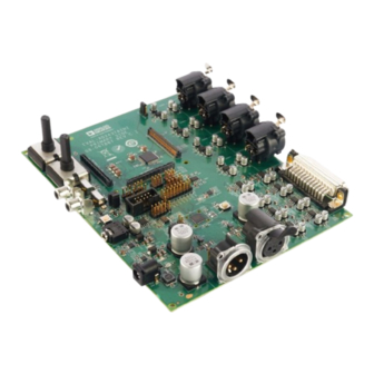
This chapter provides information on the major components and peripherals on the board, along with instructions for installing and setting up the emulation software. Product Overview The board features: • Analog Devices AD2437 - Audio Bus Transceiver • Audio • Analog Devices ADAU1452 - SigmaDSP Digital Audio Processor •... -
Page 10: Package Contents
• Universal 24V DC power supply • A B Software - Online Request Document Contact the vendor where you purchased your EVAL-AD2437A1NZ evaluation board or contact Analog Devices, Inc. if any item is missing. Default Configuration The Default Hardware Setup figure shows the default settings for jumpers and switches and the location of the jumpers, switches, connectors, and LEDs. -
Page 11: Reference Design Information
Figure 2-1: Default Hardware Setup Reference Design Information A reference design info package is available for download on the Analog Devices Web site. The package provides information on the schematic design, layout, fabrication, and assembly of the board. EVAL-AD2437A1NZ Manual... -
Page 12: Adau1452 - Sigmadsp Digital Audio Processor
(ADCs) with differential input and eight digital-to-analog converters (DACs) with differential output, using the Analog Devices, Inc., patented multibit sigma delta (Σ-Δ) architecture. An I2C port is included, allowing a microcontroller to adjust 2–4... -
Page 13: Adm6315 - Open-Drain Microprocessor Supervisory Circuit
AD1937 eliminates the need for a separate high frequency master clock and can also be used with a suppressed bit clock. The DACs and ADCs are designed using the latest Analog Devices continuous time architecture to further minimize EMI. By using 3.3 V supplies, power consumption is minimized and further reduces emissions. -
Page 14: Hardware Reference
Hardware Reference 3 Hardware Reference This chapter describes the hardware design of the EVAL-AD2437A1NZ. Switches This section describes operation of the switches. The switch locations are shown in the Switch Locations figure. EVAL-AD2437A1NZ Manual 3–1... -
Page 15: User I/O Ports ( S3)
Switches Figure 3-1: Switch Locations User I/O Ports ( S3) General purpose momentary push button connected to SIO2 with a corresponding LED. Please see PRM for SIO2 configuration. 3–2 EVAL-AD2437A1NZ Manual... -
Page 16: Reset Pushbutton ( S1)
The reset pushbutton resets the ADAU1452 and AD2437. Reset LED ( DS7) is used to indicate when the board is in reset. Connectors This section describes connector functionality and provides information about mating connectors. The connector locations are shown in the Connector Locations figure. EVAL-AD2437A1NZ Manual 3–3... -
Page 17: A 2 B ( P17And P18)
Connectors Figure 3-2: Connector Locations B ( P17and P18) 3–4 EVAL-AD2437A1NZ Manual... -
Page 18: I2C/Spi Connector ( P2 And P23)
XLR cable assembly ADAU1452 AUX Select ( P10-P13) P10-P13 are headers that can be used to interface peripherals to four of the ADAU1452's aux adc inputs. Refer to schematic for further details. Headphone DAC ( P25 ) EVAL-AD2437A1NZ Manual 3–5... -
Page 19: Spdif Output ( P19)
These connectors are I2S signals from ADAU1452 SigmaDSP. Ports allow probing or interfacing with external cus- tom boards if required. The connector is a 0.1" header. The pinout can be found in the schematic. SoM Interface Connection ( P16, P20, P15) 3–6 EVAL-AD2437A1NZ Manual... - Page 20 DAI0_PIN09 DAI0_PIN19 SPI3_MISO MLB_DATN DAI1_PIN09 DAI1_PIN19 USB_D1 USB_CLK MLB_DAT Table 3-2: SoM Interface B Connector (P20) Signal Signal Signal Signal Signal GND1 OSPI_D7 TWI2_SDA MSI_D3 LINKPORT0_D7 GND2 SPI1_SEL2b UART2_RXb GND8 LINKPORT1_D7 SP2_OSPI_MISO 23 SPI2_SEL2b UART0_TXb MSI_D4 LINKPORT0_D6 EVAL-AD2437A1NZ Manual 3–7...
- Page 21 EFCLK GND2 GND4 CLK1 PPI_D17 ~UART3_RX ETH0_MDIO ETH0_RXCTL_C PPI_CLK PPI_D06 PPI_D16 ETH1_MDIO ETH0_PTPCLKI CLK2 PPI_D18 ~UART3_RTS ETH0_MDC GND3 PPI_FS1 PPI_D07 GND11 ETH1_MDC ETH0_PTPAUX- GND8 PPI_D19 ~UART3_CTS ETH0_MD_INT ETH0_TXD3 PPI_FS2 PPI_D08 VDD_EXT ETH1_RXD1 ETH0_PTPPPS0 JTG0_TMS/ PPI_D20 SYS_FAULT SWDIO 3–8 EVAL-AD2437A1NZ Manual...
-
Page 22: Power Plug ( P14)
Part Description Manufacturer Part Number 2.1 mm power jack PJ-102AH Mating Cable 24.0VDC @3A power supply Kaga Electronics USA KTPS65-2430DT-3P-VI-C-P1 Jumpers This section describes functionality of the configuration jumpers. The Jumper Locations figure shows the jumper locations. EVAL-AD2437A1NZ Manual 3–9... -
Page 23: A2B Address Select ( Jp3 And Jp4)
Jumpers Figure 3-3: Jumper Locations A2B Address Select ( JP3 and JP4) The A2B address Select jumper will be used to choose which address is being used on A2B chip. The default address is 0X68. 3–10 EVAL-AD2437A1NZ Manual... -
Page 24: Self Discovery ( Jp1)
USBi SPI SEL ( JP2 ) Jumper option to use SPI signals from SOM module or AD2437 chip. Jumper Source Hang on 1 (DEFAULT) SCL and SDA 1 and 2 AD2437 SPI 2 and 3 SOM SPI EVAL-AD2437A1NZ Manual 3–11... -
Page 25: Ad1937 Clock Select ( P6 )
Refer to schematic for further details and jumper arrangements. Jumper Routing 1 and 2 (DEFAULT) ADAU1452 clock 2 and 3 SOM clock LEDs This section describes the on-board LEDs. The LED Locations figure shows the LED locations. 3–12 EVAL-AD2437A1NZ Manual... -
Page 26: A 2 B Interrupt ( Ds4)
Figure 3-4: LED Locations B Interrupt ( DS4) The A B interrupt LED is driven by the AD2437. The LED is turned on when the IRQ pin drives it high. Refer to the TRM for further info on using interrupts. EVAL-AD2437A1NZ Manual 3–13... -
Page 27: Adau1452 Status ( Ds1)
When ON (red), it indicates that the board is in reset. A master reset is asserted by pressing S1, which activates the LED. Power Status LED Indicator LED indication for the individual power regulation circuits. DS8: +3.3V @1.5A DS6 : +5.0V @1.5A DS9 : +24.0V @3.0A 3–14 EVAL-AD2437A1NZ Manual... - Page 28 EVAL-AD2437A1NZ Manual...
Need help?
Do you have a question about the EVAL-AD2437A1NZ and is the answer not in the manual?
Questions and answers