Table of Contents
Advertisement
Quick Links
Advertisement
Table of Contents

Related Manuals for Humandata EDX-008


Summary of Contents for Humandata EDX-008
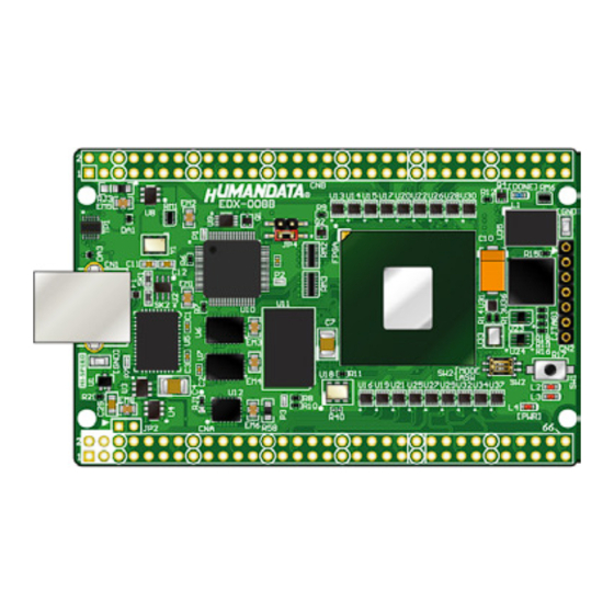
- Page 1 Kintex-7 USB-FPGA Board EDX-008 Series User’s Manual Ver. 1.1 HuMANDATA LTD.
-
Page 2: Table Of Contents
Table of Contents Revision History ....................1 Introduction ....................1 1. Specifications ..................... 2 2. Overview ......................3 2.1. Name of Parts .......................3 2.2. Block Diagram ......................4 2.3. Clock ........................4 2.4. MRAM ........................4 2.5. Power Supply ......................5 2.6. VIO(B) Setting Jumper ..................5 2.7. - Page 3 HuMANDATA will revise the diagram. When a problem can be solved only by replacing components or modifying the product, HuMANDATA will take back the product to replace it with a properly functioning product.
-
Page 4: Revision History
[MT41K64M16TW-107:J] Introduction Thank you for purchasing our product EDX-008. EDX-008 is an evaluation board with USB interface equipped with a Xilinx FPGA Kintex-7 series and FTDI's FT2232H. By using the original configuration tool “BBC[EDX-008]”, no download cable or Xilinx developing environment is needed to configure FPGA and configuration device on the board. -
Page 5: Specifications
3.386" x 2.126" (86 x 54 [mm]) Weight 30 [g] typ. SIL 7-pin header (Mounted) x1 DIL 80-pin header (Cuttable) x 2 Accessories USB cable (1.8m) x1 RoHS Compliance * There may be cases that these parts and specifications are changed. EDX-008 Series v1.1... -
Page 6: Overview
2. Overview 2.1. Name of Parts VIO(B) DONE LED Setting Jumper Config. Device FT2232H Setting Jumper MRAM JTAG Oscillator DDR3 SDRAM User LED Oscillator User SW Setting SW Component Side User I/O (CNB) User I/O (CNA) Solder Side EDX-008 Series v1.1... -
Page 7: Block Diagram
For more detail, please refer to circuit schematics. 2.4. MRAM MRAM is a non-volatile memory and is able to read/write in almost unlimited times. So it is very convenient and can be used as RAM and also ROM. EDX-008 Series v1.1... -
Page 8: Power Supply
VCCOA (3.3V). Bank Group B is fixed to VCCOA. But it can be changed by setting RJ3. For more details, please refer to the circuit schematics. VCCOB is powered by on-board 3.3V (VCCOA) (Factory Setting) RJ3[1-2] VCCOB is powered by CNB (external input) RJ3[2-3] EDX-008 Series v1.1... -
Page 9: Ft2232H Setting Jumper
For each pins details and other modes setting, please refer to Kintex-7 configuration user guide. Configuration Mode X_MODE ASW2 User Master SPI User Slave Serial * ON: Low level Master SPI : for use Configuration Device Slave Serial : for use JTAG or BBC[EDX-008] EDX-008 Series v1.1... -
Page 10: Fpga Configuration
3. FPGA Configuration 3.1. Using Original Tool By using the original configuration tool “BBC[EDX-008]”, the following function is available without download cable. FPGA configuration ● Write and Erase configuration device ● “BBC[EDX-008]” is available for free from a support page. -
Page 11: Using Configuration Device
4. Device Driver To recognize USB controller, installing device driver is needed. The first time EDX-008 is connected to a PC, installing it is required by Operation System. The device driver is available at the support page. EDX-008 Series v1.1... -
Page 12: Factory Setting Of Ft2232H Eeprom
5. Factory Setting of FT2232H EEPROM Factory presetting is as follows. The other items are not changed from the default. EDX-008 Series v1.1... -
Page 13: Documentation And User Support
6. Documentation and User Support The following documents and other supports are available at http://www.hdl.co.jp/en/spc/EDX/edx-008/ Circuit Schematic Pin List Dimensional drawing Net List Original Configuration Tool “BBC[EDX-008]” Device Driver … and more. EDX-008 Series v1.1... - Page 14 Kintex-7 USB-FPGA Board EDX-008 Series User’s Manual Ver. 1.1 ..........Jun. 9, 2017 HuMANDATA LTD. Address: 1-2-10-2F, Nakahozumi, Ibaraki Osaka, Japan ZIP 567-0034 Tel: 81-72-620-2002 (Japanese) Fax: 81-72-620-2003 (Japanese/English) URL: http://www2.hdl.co.jp/en/ (Global) http://www.hdl.co.jp/ (Japan)
Need help?
Do you have a question about the EDX-008 and is the answer not in the manual?
Questions and answers