Table of Contents
Advertisement
Quick Links
Advertisement
Table of Contents

Related Manuals for Humandata XCM-209 Series


Summary of Contents for Humandata XCM-209 Series
- Page 1 Kintex-7 FFG900 FPGA Board XCM-209 Series User’s Manual Ver. 1.0 HuMANDATA LTD.
-
Page 2: Table Of Contents
Table of Contents Revision History ....................1 Introduction ....................1 1. Shared Pins [IMPORTANT] ................2 2. Specifications ..................... 3 3. Overview ......................4 3.1. Name of Parts .......................4 3.2. Block Diagram ......................5 3.3. Power Supply ......................6 3.4. User I/O (CNA, CNB, CNC, CND) ..............6 3.5. - Page 3 HuMANDATA will revise the diagram. When a problem can be solved only by replacing components or modifying the product, HuMANDATA will take back the product to replace it with a properly functioning product.
-
Page 4: Revision History
Thank you for purchasing our product XCM-209. This is an evaluation board equipped with a Xilinx FPGA Kintex-7, power, reset, and clock circuit and configuration device. It can provide you with very convenient and easy-to-use development environment. XCM-209 Series v1.0... -
Page 5: Shared Pins [Important]
To prevent these pins from being shorted out, it is recommended to set them as “Float” in advance. Please refer to the following steps and check the “Unused IOB Pins” setting. 1. Open [Implementation Design], then open [Bitstream Settings] 2. Open [additional bitstream settings], and confirm [Unused IOB Pins] setting. XCM-209 Series v1.0... -
Page 6: Specifications
3.386" x 2.126" (86 x 54 [mm]) Weight 50 [g] typ. SIL 7-pin header (Mounted) x 1 FX10A-80S/8-SV x 2 Accessories FX10A-100S/10-SV x 2 (Hirose Electric) Spacer x 4 RoHS Compliance * There may be cases that these parts and specifications are changed. XCM-209 Series v1.0... -
Page 7: Overview
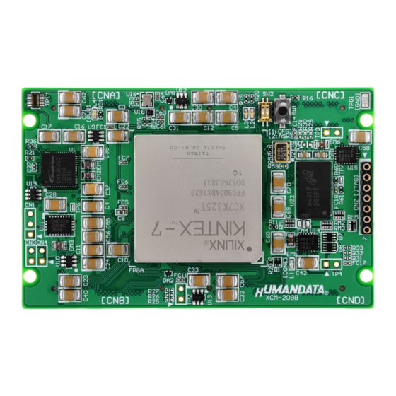
User LED Config. SW User SW Oscillator Power LED Oscillator JTAG Debug I/F DDR3SDRAM FPGA Done LED Component Side User I/Os (CNC) User I/Os (CNA) Lebel Converters Config. Device User I/Os (CNB) User I/Os (CND) Solder Side XCM-209 Series v1.0... -
Page 8: Block Diagram
1 .8V, 2.0V Power LED (3.3V) 148 GPIO U s er I/Os CNB U s er I/Os CND V IO(B) INPUT E xt . Clock (Option) V IO(D) INPUT E xt . Clock (Option) X CM-209 Rev.A XCM-209 Series v1.0... -
Page 9: Power Supply
A DIP switch (SW2[2]) is also pulled up, so you can input low level signal to the FPGA when you slide it to ON. 3.7. Debug I/F 3-pin interface (CN1) can be used for any purpose. They are connected through series resisters to FPGA pins. XCM-209 Series v1.0... -
Page 10: Configuration Switch
This connector is used to configure the FPGA and program the configuration device in-system. Pin assignment is as follows. You can use Xilinx download cable. Pin No. Signal Name Direction Notice Please pay attention not to attach cables in reverse. XCM-209 Series v1.0... -
Page 11: Fpga Configuration
Select your bit file, and generate MCS file. 5.2. Programming Configuration Device Select a recognized device name from [Tools - Add Configuration Memory Device] window. Select n25q128 (or 256) -3.3v-spi-x1_x2_x4 for memory name. Select an mcs file and operation command then click [OK]. XCM-209 Series v1.0... -
Page 12: Additional Documentation And User Support
6. Additional Documentation and User Support The following documents and other supports are available at http://www.hdl.co.jp/en/spc/XCM/xcm-209/ Circuit Schematic Pin List Outline drawing Net List … and more. XCM-209 Series v1.0... - Page 13 Kintex-7 FFG900 FPGA Board XCM-209 Series User’s Manual Ver. 1.0 ..........Apr. 14, 2017 HuMANDATA LTD. Address: 1-2-10-2F, Nakahozumi, Ibaraki Osaka, Japan ZIP 567-0034 Tel: 81-72-620-2002 (Japanese) Fax: 81-72-620-2003 (Japanese/English) URL: http://www2.hdl.co.jp/en/ (Global) http://www.hdl.co.jp/ (Japan)
Need help?
Do you have a question about the XCM-209 Series and is the answer not in the manual?
Questions and answers