Table of Contents
Advertisement
Quick Links
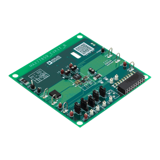
MAX77859 Evaluation Kit
General Description
The MAX77859 evaluation kit (EV kit) is a fully
assembled and tested printed circuit board (PCB)
that demonstrates the MAX77859, a high-efficiency,
high-performance buck-boost regulator with a peak
switching current of 7.8A. It supports USB Type-C PPS
requirements
with
programmable
(20mV/step) and programmable output current limit
(50mA/step). The IC is capable of 2.5V to 22V input and
dynamically
adjustable
interface) between 3.2V to 16V (internal feedback) or
between 3V to 20V (external feedback). The EV kit is
factory-configured as internal feedback with a default
startup output voltage of 5V. Other startup voltages can be
achieved with external feedback resistors.
I/O pins are available to support the I
enable function, forced-PWM mode, and interrupt/power-
2
OK indicator. The I
C target address, switching current
limit, and feedback configuration can be adjusted by
changing the R
resistor (R9). MAXUSB_INTERFACE#
SEL
allows the use of Windows
graphical user interface (GUI) as well as a detailed
register-based interface to exercise all features of the IC.
The EV kit is compatible with any version of the MAX77859
WLP IC (MAX77859AEWO+T is the default one installed).
Check List
•
MAX77859 IC Evaluation Board
•
MAXUSB_INTERFACE# (USB-to-I
•
USB Type-A to Micro-USB Cable
•
Windows-based Graphical User Interface (GUI) Software
• Can be downloaded from the Analog Devices website at
Tools & Simulation tab). Windows 7 or newer is required to use the EV kit GUI software.
EV Kit Specifications
SPECIFICATION
Input voltage
Output voltage
Default output voltage
Switching current limit
Peak efficiency
USB Type-C is a registered trademark of USB Implementers Forum.
Windows is a registered trademark and registered service mark of Microsoft Corporation.
© 2023 Analog Devices, Inc. All rights reserved. Trademarks and registered trademarks are the property of their respective owners.
O n e A n al og W ay, W il mi ngton , MA 01887 U.S.A. | T el: 781. 329. 4700 | © 20 2 3 Analog Devic es, I nc. Al l ri ghts res erv ed.
output
voltage
2
output
(through
I
C
2
C serial interface,
®
-based software with a friendly
2
C Serial Interface)
TEST CONDITION
Internal feedback
External feedback
Internal feedback
V
= 7.6V, V
= 9V, 1500mA load
IN
OUT
Evaluates: MAX77859 (WLP)
Features
•
Proven PCB Reference Design and Layout Benefit
•
Fully Assembled and Tested
•
Sense Points for High-Accuracy Measurements
•
Accessible Test Point Pins for EN, FPWM,
POKB/INTB, V
•
MAXUSB_INTERFACE# Allows Easy Communication
with a Windows PC
•
GUI Software that Drives I
serial
Optional Software Control
•
Startup Output Voltage Adjustable Through External
Feedback Resistors
•
Output Voltage and Output Current Limit Dynamically
Adjustable Through I
•
2
I
C Target Address, Switching Current Limit, and
Feedback Configuration Adjustable Using R
Ordering Information
https://www.analog.com/MAX77859WEVKIT
2
, and I
C Serial Interface SCL, SDA
IO
2
C Serial Interface for
2
C Serial Interface
appears at end of data sheet.
MIN
TYP
MAX
2.5
22
3.2
16
3
20
5
7.8
96.0
319-100993; Rev 0; 4/23
(R9)
SEL
(under the
UNIT
V
V
V
A
%
Advertisement
Table of Contents

Related Manuals for Analog Devices MAX77859


Summary of Contents for Analog Devices MAX77859
- Page 1 319-100993; Rev 0; 4/23 © 2023 Analog Devices, Inc. All rights reserved. Trademarks and registered trademarks are the property of their respective owners. O n e A n al og W ay, W il mi ngton , MA 01887 U.S.A. | T el: 781. 329. 4700 | © 20 2 3 Analog Devic es, I nc. Al l ri ghts res erv ed.
- Page 2 C INTERFACE AGND PGND *CHOOS E R VALUE SEL * BASED ON TABLE 2 Figure 1. MAX77859 Typical Application Circuit SWITCH NODES PROBE POINTS INPUT SUPPLY TERMINALS OUTPUT LOAD TERMINALS INPUT VOLTAGE SENSE PINS OUTPUT VOLTAGE SENSE PINS MAX77859 SOLUTION...
-
Page 3: Quick Start
C serial interface (optional) • USB Type-A to Micro-USB cable (optional) • Windows-based PC with MAX77859 EV kit GUI (optional) Setup Overview Typical bench setups for the MAX77859 EV kit with different configurations are shown in Figure Figure 4, and Figure www.analog.com... - Page 4 MAX77859 Evaluation Kit Evaluates: MAX77859 (WLP) PGND1S PGND2S PGND1 PGND2 DIGITAL DC POWER ELECTRONIC DIGITAL VOLTMETER SUPPLY LOAD VOLTMETER MAX77859 EV KIT OUTS J1: INSTALLED 1-2 J2: INSTALLED Figure 3. EV Kit Connection Block Diagram—Standalone Operation PGND1S PGND2S PGND1 PGND2...
-
Page 5: Standalone Operation
V pin. This is useful for systems without a host controller or if the MAX77859 is the only power supply in the system. To configure the MAX77859 EV kit for standalone operation, install header jumper www.analog.com... - Page 6 Warning: Make sure the external I C serial bus’s logic voltage level is compatible with the MAX77859’s I/O logic voltage level (2.0V max). Refer to the MAX77859 IC data sheet for more information regarding the I/O logic voltage level. Configuration Resistor The MAX77859 includes an SEL pin to set the I C target address, switching current limit, and feedback configuration.
- Page 7 *Default EV kit configuration High-Temperature Testing The MAX77859 is rated for operation under junction temperatures up to +125°C. Note that not all components on the EV kit are rated for temperatures this high. Some ceramic capacitors experience extra leakage when put under temperatures higher than they are rated for and supply current readings for the IC might be larger than expected.
-
Page 8: Input Voltage
MAX77859 Evaluation Kit Evaluates: MAX77859 (WLP) ambient or junction temperatures. Consider replacing these components if IC operation at +125°C ambient or junction temperature is an important use case. List of capacitors not rated for +125°C: C1 (IN bulk capacitor), C10, C11 (OUT capacitors) Critical Node Measurement (OUT and LX) The EV kit comes with probe points for measuring critical nodes OUT1, LX1, and LX2. -
Page 9: Installation
MAXUSB_INTERFACE# drives I C communication with the EV kit. Every control in the GUI corresponds directly to a register within the MAX77859. Refer to the Register Map section of the MAX77859 IC data sheet for a complete description of the registers. See Figure 7 for a screenshot of the GUI upon first opening. - Page 10 Current Limit Configuration (MAX77859A Only), and Miscellaneous Configurations. Click Read Once located on the top of the GUI window to obtain all setting values currently stored on all the MAX77859’s registers. After changing the setting values in the GUI software, click Write on the top of the GUI window to apply all settings to the MAX77859’s registers.
- Page 11 (using the internal reference voltage DVS slew rate). Refer to the MAX77859 IC data sheet for more information on each available setting. Click Read to obtain the setting stored on the IC and click Write to apply new settings to the IC.
- Page 12 Careful circuit board layout is critical to achieving low switching power losses and clean, stable operation. The EV kit serves as a recommended layout for the MAX77859. A high-density interconnect (HDI) PCB is required to route to the EN, FPWM, SEL, and SRP pins.
-
Page 13: Ordering Information
MAX77859 Evaluation Kit Evaluates: MAX77859 (WLP) LEGEND LAYOUT BASED ON USING INTERNAL 7.8A I FEEDB ACK RESISTORS CONFIGURATION 5.48mm x 5.28mm 5.48mm x 5.28mm PGND PGND 1206 0805 BST1 BST2 0603 0603 0603 POKB/INTB 0402 8mil HOLE, 16mil PAD 0402... - Page 14 CAPACITOR; SMT (0402); OPEN; OPEN FORMFACTOR RESISTOR; 0402; OPEN; R11, R14 OPEN FORMFACTOR Components below this line are outside of the immediate MAX77859 evaluation circuit and solution silkscreen. AGND1, AGND2, IN, EVK KIT PARTS; MAXIM PAD; WIRE; MAXIM OUT, 9020 BUSS WEICO WIRE NATURAL;...
- Page 15 MAX77859 Evaluation Kit Evaluates: MAX77859 (WLP) SULLINS CONNECTOR; FEMALE; MINI SHUNT; EV_KIT_BOX NPC02SXON-RC ELECTRONICS 0.100IN CC; OPEN TOP; JUMPER; CORP. STRAIGHT; 2PINS TEST POINT; PIN DIA=0.1IN; TOTAL INS, LX-1, LENGTH=0.3IN; BOARD LX-2, OUTS, 5000 KEYSTONE HOLE=0.04IN; RED; PHOSPHOR VIO, VL BRONZE WIRE SILVER PLATE FINISH;...
- Page 16 MAX77859 Evaluation Kit Evaluates: MAX77859 (WLP) SWITCH; SPST; SMT; STRAIGHT; 219- 20V; 0.1A; SURFACE MOUNT DIP 219-3MST 3MST SWITCH-AUTO PLACEABLE; RINSULATION=1000M OHM MODULE; BOARD; MAX32625PICO MAX32 BOARD DESIGN FOR MAX32625 MAX32625PICO MAXIM 625PIC ARM CORTEX-M4F; BOARD; LAMINATED PLASTIC WITH COPPER CLAD;...
- Page 17 MAX77859 Evaluation Kit Evaluates: MAX77859 (WLP) MAX77859 EV Kit Schematic www.analog.com Analog Devices | 17...
- Page 18 MAX77859 Evaluation Kit Evaluates: MAX77859 (WLP) MAX77859 EV Kit PCB Layout MAX77859 EV Kit Component Placement Guide—Top MAX77859 EV Kit PCB Layout—Internal 2 Silkscreen MAX77859 EV Kit PCB Layout—Top View MAX77859 EV Kit PCB Layout—Internal 3 www.analog.com Analog Devices | 18...
- Page 19 MAX77859 Evaluation Kit Evaluates: MAX77859 (WLP) MAX77859 EV Kit PCB Layout (continued) MAX77859 EV Kit PCB Layout—Internal 4 MAX77859 EV Kit PCB Layout—Bottom View MAX77859 EV Kit PCB Layout—Internal 5 MAX77859 EV Kit PCB Layout—Bottom Silkscreen www.analog.com Analog Devices | 19...
-
Page 20: Revision History
Information furnished by Analog Devices is believed to be accurate and reliable. However, no responsibility is assumed by Analog Devices for its use, nor for any infringements of patents or other rights of third parties that may result from its use. Specifications subject to change without notice. No license is granted by implication or otherwise under any patent or patent rights of Analog Devices.
Need help?
Do you have a question about the MAX77859 and is the answer not in the manual?
Questions and answers