Table of Contents
Advertisement
Quick Links
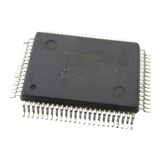
TOSHIBA CMOS Digital Integrated Circuit Silicon Monolithic
Single-Chip DTS Microcontroller (DTS-22)
TC9314F is a 4 bit CMOS microcontroller for single-chip digital
tuning systems with built-in prescaler, PLL and LCD driver.
The CPU has 4 bit parallel addition/subtraction (eg, AI and SI
instructions), logical operations (eg, OR and AN), several bit
judge and compare instructions (eg, TM and SL), and time base
functions.
The device is in an 80 pin mini flat package. It includes
abundant I/O ports controlled by powerful input and output
instructions (IN1-3, OUT1-3) exclusive key input ports, abundant
LCD output ports, interrupts, a BUZR port, 6 bit A/D and D/A
converters, serial interface, and IF counter.
With CMOS architecture for low power consumption, TC9314F
is ideal for providing digital tuning for multiband radios,
radio-cessatte players and other portable equipment.
Features
4 bit microcontroller for single-chip digital tuning systems
Operating voltage V
DD
On-chip prescaler (fixed to 1/2 frequency division +2-modulus prescaler: fmax
1/3-duty, 1/2-bias driven LCD driver, with on-chip 3 V constant-voltage display circuit
Easy backup of data memory (RAM) and various ports
Program ROM: 16 bits × 6144 steps
Data memory (RAM): 4 bits × 384 words
Powerful instruction set with 54 1-word instructions
Instruction execution time of 40 µs (75 kHz crystal connected; 80 µs for MVGS and DAL instructions)
4 add and 4 subtract instructions
Note 1: This device is vulnerable to surge voltage. Take it into account when using this device in your system.
Powerful compound judge instructions (TMTR, TMFR, TMT, TMF, TMTN and TMFN)
Data transfer at the same row address (MVSR instruction)
Register indirect transfer available (MVGD and MVGS instructions)
16 powerful general registers assigned in RAM
Stack levels: 4
No concepts of pages or fields in program ROM. Features 6144 steps that allow JUMP or CAL instructions at
any point.
16 bit contents of any address in 1024 steps of the program ROM can be referenced freely. (DAL instruction)
Independent FM
and AM
IN
and DO2).
Choice of seven reference frequencies by program
Powerful input and output instructions (IN1~3 and OUT1~3)
Input-only ports (K0~K3) for key inputs and 33 LCD drive pins (90 segments maximum).
26 I/O ports (16 ports specifiable in units of bits, 10 output-only ports). Three pins (IF
be switched using instructions for use as input-only ports IN1 and IN2, and output-only port OT2, respectively.
In addition LCD output pins S19~S30 can be switched to I/O ports in units of bits.
2 external interrupt input ports.
These are able to switch for use as general input ports by program.
TC9314F
of 2.7~5.5 V, with CMOS architecture for low power consumption
pins for FM and AM frequency input and two phase comparison outputs (DO1
IN
Weight: 1.57 g (typ.)
1
TC9314F
130 MHz)
, IF
and DO2) can
IN1
IN2
2003-07-03
Advertisement
Table of Contents

Subscribe to Our Youtube Channel
Related Manuals for Toshiba TC9314F


Summary of Contents for Toshiba TC9314F
- Page 1 TOSHIBA CMOS Digital Integrated Circuit Silicon Monolithic TC9314F Single-Chip DTS Microcontroller (DTS-22) TC9314F is a 4 bit CMOS microcontroller for single-chip digital tuning systems with built-in prescaler, PLL and LCD driver. The CPU has 4 bit parallel addition/subtraction (eg, AI and SI...
-
Page 2: Pin Assignment (Top View)
TC9314F Three backup modes can be implemented using instructions: CPU operation only, clock generation only or clock stop. Features a built-in 2 Hz timer flip-flop and 10/100 Hz interval pulse output (internal time-based port) Detection of PLL locked state supported. -
Page 3: Block Diagram
TC9314F Block Diagram 2003-07-03... -
Page 4: Pin Function
TC9314F Pin Function Pin No. Symbol Pin Name Function and Operation Remarks Common output pins for the LCD panel. Can COM1 display up to 90 segments in a matrix with S1-S30. LCD common Three value levels, V , 1/2 V... - Page 5 TC9314F Pin No. Symbol Pin Name Function and Operation Remarks 4 bit I/O port. Input or output can be programmed for each bit. Pins P3-0 through P3-2 serve as the analog inputs and outputs for the built-in A/D and D/A converters.
- Page 6 TC9314F Pin No. Symbol Pin Name Function and Operation Remarks Input pin for controlling test mode. When the pin is high, test mode; when low, normal Test mode control TEST operation. input Normally used low or in the NC state. (pull-down resistance built in) Input pin used to request/cancel a hold state.
- Page 7 TC9314F Pin No. Symbol Pin Name Function and Operation Remarks Pin for applying the power supply. Normally, a V of 2.7~5.5 V is applied during PLL operation. When PLL is stopped, a V 1.8~5.5 V is applied. During backup (at execution of the CKSTP instruction), voltage can be reduced to 1.2 V.
- Page 8 TC9314F Pin No. Symbol Pin Name Function and Operation Remarks Crystal oscillator pin. A 75 kHz reference crystal oscillator is connected to the X and X pins. Oscillation stops during execution of a CKSTP Crystal oscillator pin instruction. The V pin is the power supply for the crystal oscillator.
-
Page 9: Explanation Of Operation
TC9314F Explanation of Operation CPU is composed of program counter, stack register, ALU, program memory, data memory, G-register, carry F/F and judging circuit. 1. Program Counter (PC) Program Counter is a block to designate the address of program memory (ROM), and is composed of 13 bits binary up counter. -
Page 10: Data Memory (Ram)
TC9314F 5. Data Memory (RAM) Data memory is composed of 4 bit 384 words and used for storing data. This 384 words are expressed with row address (5 bits) and column address (4 bits). 320 words (row address 04H~17H) among the data memory are indirect addressing by G-register. For... - Page 11 TC9314F 7. Data Register (DATA REG.) This is a register composed of 1 16 bits. In this register, 16 bits data of optional address among the program memory is loaded during executing of DAL instruction. This register is treated as one of the port, and when KEY instruction among input and output instruction is executed, it’s content is read in the data...
- Page 12 TC9314F 11. Explanation List of Function and Operation of Instructions (explanation of symbols) M: Data memory address Normally, one of 000H~03FH address of data memory. M*: Data memory address (256 word) One of 000H~0FFH address of data memory (available at executing ST and LD instruction) r: General register One of 00H~0FH address of data memory.
- Page 13 TC9314F Machine Language (16 bit) Mnemonic Explanation of Function Explanation of Operation (6 bit) (2 bit) (4 bit) (4 bit) Add immediate data to M, I 000000 memory Add immediate data to M, I 000001 memory with carry Add memory to general...
- Page 14 TC9314F Machine Language (16 bit) Mnemonic Explanation of Function Explanation of Operation (6 bit) (2 bit) (4 bit) (4 bit) Load memory to general r, M* (M*) 0101 register (4 bit) Store general register to M*, r 0110 memory (4 bit)
- Page 15 TC9314F Machine Language (16 bit) Mnemonic Explanation of Function Explanation of Operation (6 bit) (2 bit) (4 bit) (4 bit) Test general register bits by memory bits, then skip TMTR r, M Skip if r [N (M)] all “1” 010000...
- Page 16 TC9314F I/O Map All the ports in the device are accessed by the six input/output instructions (OUT1~OUT3 and IN1~IN3) using the 4 bit code number matrices. The I/O map on the following page shows the port allocation. Horizontally, the I/O map shows the ports manipulated by each input/output instruction.
- Page 17 TC9314F I/O Map OUT1 OUT2 OUT3 Code IF offset DA/AD control I/O port 1 IF control I/O port 1 DCREF ON AD1 ON AD2 ON DA ON BUSY MANUAL OVER Programmable counter DA REF data 1 I/O port 2 IF data...
- Page 18 TC9314F Connecting Crystal Oscillator The following diagram shows the connection of the 75 kHz crystal oscillator to the device’s crystal oscillator pins (X The oscillation signal is supplied to the clock generator, reference frequency divider, and other sub-systems to generate the various CPU timing signals, reference frequency, and other signals. The power supply for the crystal oscillator circuit is the voltage (V 1.5 V typ.) supplied by the built-in constant voltage circuit.
-
Page 19: Backup Modes
TC9314F Backup Modes To enter the three backup modes, execute the CKSTP or WAIT instruction. 1. Clock Stop Mode Clock stop mode halts the system and maintains the internal state of the system immediately prior to halting. During a halt, the system is maintained with low current consumption (1 A or below, at V V). - Page 20 TC9314F Clock stop mode timing MODE-0 (Executing the CKSTP instruction while the HOLD pin input is low sets the device to clock stop mode.) MODE-1 (Executing the CKSTP instruction always sets the device to clock stop mode.) Circuit example (MODE-0)
-
Page 21: Wait Mode
TC9314F 2. Wait Mode Wait mode halts the system and maintains, with reduced current consumption, the internal state of the system immediately prior to halting. Two wait modes are available: “soft wait” and “hard wait”. When the WAIT instruction is executed, execution halts at the address of the WAIT instruction. Therefore, when wait mode is released, execution starts again from the next instruction without delaying for the standby time. - Page 22 TC9314F Programmable Counter The programmable counter block consists of a 2-modulus prescaler, 4 bit and 12 bit programmable counters, and the ports used to control the block. The programmable counters can be turned on and off by the contents of the reference ports.
- Page 23 TC9314F 3. IF Correction Function for FM Band When the pulse swallow method is selected, the IF 1 ports allow the actual divisor to be varied by 1 without changing the programmed divisor. This can be used for IF offset in FM.
-
Page 24: Reference Port
TC9314F Direct division method circuit structure This circuit bypasses the prescaler and uses the 12 bit programmable counter. Note 26: The FM and AM pins incorporate amps. Connecting a capacitor permits low-amplitude operation. The input pins not selected by the division method are pulled down. In PLL off mode (set by the reference port), the inputs are also pulled down. - Page 25 TC9314F Phase Comparator, Clock Detection Port The phase comparator compares the reference frequency signal supplied by the reference frequency divider with the divided signal output by the programmable counter, and outputs the phase difference. The output of the phase comparator is used to control the VCO via the low pass filter so as to eliminate the frequency and phase difference between the two signals.
- Page 26 TC9314F The OTC, OT, and Hz control bits of the DO2 control port set the DO2 output pin as a general-purpose output port, and control whether DO2 goes to high impedance instead of outputting the phase difference. Set these bits to the required values by program.
- Page 27 TC9314F 3. Phase Comparator, Unlock Port Circuit Structure When Setting Different Filter Constants When Using the Same Low Pass Filter for for Each Band Both Bands (set DO2 to high impedance to switch the filter constant) 2003-07-03...
- Page 28 TC9314F IF Counter This is a 20 bit general-purpose intermediate frequency (IF) counter used for such purposes as counting the FM or AM intermediate frequency during auto-tuning or detecting the auto-stop signal. The IF counter also has a period measuring function for measuring the period of low-frequency pilot signals, for example.
- Page 29 TC9314F Note 29: When the PLL is off, the IF counter is disabled. (When the timer/counter is in use, the IF counter is enabled.) IF counter auto mode (frequency measuring) To use IF counter auto mode, use the switching bit to set the IF pin to IF input, and set the bit to frequency measuring mode “0”.
- Page 30 TC9314F Timer/counter mode When not using the IF counter, the block can be used as a timer or binary counter. Set the MANUAL, G0, and G1 bits to “1” to start binary counting using the 75 kHz frequency as the reference clock.
-
Page 31: Lcd Driver
TC9314F LCD Driver The LCD driver has a 1/3 duty and 1/2 bias drive (frame frequency is 167 Hz). The common outputs are at three voltages: V /2, and GND. The segment outputs are at two voltages: V and GND. - Page 32 TC9314F The LCD driver control ports consist of a segment data selection port and segment data ports. Use the = DH~FH] to access these ports. The LCD driver can operate as an OUT2 instruction with the operand [C I/O port under the control of the SEG I/O control bit (φL2F). Setting the bit to “1” sets segment output.
- Page 33 TC9314F 3. LCD Driver Timing Chart The following chart shows the timing for the COM1~COM3 output waveforms and the eight types of segment output waveform. 2003-07-03...
- Page 34 TC9314F 4. Example of Timing Chart for LCD Driver Output Data and Loading Key Data The following chart shows the output waveform timing and key return data loading timing when the common and segment outputs are allocated as shown. The voltages output in the LCD driver waveform are V , GND, and an intermediate voltage halfway between the two.
- Page 35 TC9314F Key Input, Key Scan Timing The following are the two basic methods of loading key data. Use software to set the key timing output port (port pins T0~T7) as the key source. Use hardware to set the LCD segment outputs (S30/KR ~S23/KR ) as the key source.
- Page 36 TC9314F 3. Key Scan Digit No. Port This port monitors the key scan operating state when loading key data using the key return signals from the LCD segment outputs (S30/KR ~S23/KR Key Scan Digit No. 4. Key Scan Data Input Port...
- Page 37 TC9314F 5. Key Matrix Structure The key matrix can have one of the following two structures. Key data loading by software (software scan) When loading key data by software, use a key matrix with the above structure. This structure allows up to 32 (4 × 8) keys to be used. The key data can be loaded at high speed. Also, as the structure has a high resistance in the N channel FETs of pins T0~T7, there is no need to use a diode to prevent reverse current flow caused by, for example, multiple keys being pressed.
- Page 38 TC9314F Key data loading by LCD segment output (hardware scan) Note 39: A key matrix to 4 × 8 = 32 can be created. Note 40: The same key line cannot contain both push keys and diode jumpers or alternate switches. Place diode jumpers or alternate switches on the key return signal output side.
-
Page 39: Serial Interface
TC9314F Serial Interface The serial interface is a serial I/O port for receiving and sending 4 bit or 8 bit data in sync with either an internal or external serial clock. The interface uses the SI, SO, and SCK pins. The interface can be used to communicate with devices such as microcontrollers or other LSIs. - Page 40 TC9314F The serial interface control and serial data can be accessed by the IN2 and OUT2 instructions with operands [C = 3H~6H]. The serial interface pins can also function as I/O port 4 pins: P4-0, P4-1, and P4-2. Setting the SIO ON bit to “1”...
- Page 41 TC9314F • When edge = “1” When the edge bit is set to “1”, the data are output from SO on the falling edge of the SCK clock. The SI input is also input to the shift register on the falling edge of the SCK clock.
- Page 42 TC9314F This method works as follows. To transmit data, the data are set in the serial output data port and SIO is performed. To receive data, the SO pin is set to input and SIO is performed. Then, the data can be loaded to data memory from the serial input data port.
- Page 43 TC9314F 3. Serial Interface Timing When SCK is set for the internal clock, the frequency of the clock output from the SCK pin is 37.5 kHz (duty: 50%). The following chart is an example of the serial interface timing. x: Undefined...
-
Page 44: Interrupt Function
TC9314F Interrupt Function INTR1 and INTR2 are the input pins for the external interrupts. These pins can also be used for remote control signal input and tape running detection input. The pins can also be set as general-purpose input ports by software. - Page 45 TC9314F 2. Interrupt Circuit Structure The interrupt circuit consists of the interrupt input circuit, interrupt counter circuit, interrupt flip-flop, interrupt enable flip-flop, interrupt detector circuit, and an interrupt control port located in an internal I/O port used to control these circuits.
- Page 46 TC9314F Interrupt enable flip-flops (IEF1, IEF2) The interrupt enable flip-flops 1 and 2 are flags to enable or disable acceptance of interrupts 1 and 2, respectively. To set interrupt enable 1 flip-flop (IEF1) to “1”, set the INTS1 bit to “1”, or execute the RN instruction with INTE1 set to “1”.
- Page 47 TC9314F • INTS1 ......Interrupt 1 enable flip-flop setting bit Setting the INTS1 bit to “1” sets the interrupt 1 enable flip-flop (IEF1) and enables the acceptance of an interrupt. The normal method of setting the interrupt 1 enable flip-flop to “1” to enable the interrupt is to execute the RN instruction with the INTE1 bit set to “1”.
-
Page 48: Interrupt Processing
TC9314F Interrupt 1 Interrupt 2 Timer Interval Timer Interval Prohibited Prohibited 0.12~ [ms] 0.12~ [ms] 0.3~ [ms] 0.1~ 0.5~ [ms] 0.2~ 0.7~ [ms] 0.3~ 0.9~ [ms] 0.4~ 1.1~ [ms] 0.5~ 1.3~ [ms] 0.6~ 1.5~ [ms] 0.7~ ・ ・ ・ ・... - Page 49 TC9314F Buzzer Output (BUZR) The buzzer output is used for such purposes as audible alarms or to issue confirmation beeps for key-presses or tuning scan mode. The buzzer frequency can be set as desired. 50% duty waveform is output. 1. BUZR Data Port The BUZR output can also be used as the OT1 output port.
-
Page 50: A/D And D/A Converter
TC9314F A/D and D/A Converter TC9314F incorporates a software-controlled successive approximation 6 bit A/D converter and a 6 bit D/A converter. The A/D and D/A converters share pins with I/O port 3. Pin operation is set by the DA/AD control port (φL20). - Page 51 TC9314F 1. A/D, D/A Converter Control Port, Data Port 2003-07-03...
- Page 52 TC9314F 2. A/D Converter The 6 bit resolution A/D converter is used for such purposes as measuring field intensity and battery voltage. The A/D analog input can be multiplexed to the two external A/D analog inputs (pins AD ), and can also be switched to the internal 1.5 V constant voltage (V ).
- Page 53 TC9314F 3. D/A Converter The D/A converter can be used for such applications as an electronic volume control that operates using analog voltage control. When using the D/A converter, set the DA ON bit to “1”, set the SEL0 bit to “0”, and set the SEL1 bit to “1”.
-
Page 54: Input/Output Ports
TC9314F Input/Output Ports 1. I/O Ports − − − − 1, − − − − 2, − − − − 3, − − − − 4, − − − − 5, − − − − 6, and − − − − 7 I/O ports −1, −2, −3, −4, −5, −6, and −7 are 4 bit ports. - Page 55 TC9314F 2. Key Timing Output Port T0~T7 form an 8 bit output port. When forming a key matrix by software, this port outputs the key timing signal. Accordingly, the N channel FET output has a high resistance to minimize the sink current. Therefore, when using these pins as standard output ports, be careful of the type of circuit being driven.
- Page 56 TC9314F Register Port The G register (mentioned in the CPU description) and the data register are treated as internal ports. 1. G Register (φ φ φ φ L1D~φ φ φ φ L1E) = 04H~17H) in data memory for the MVGD and MVGS This register sets the row address (D instructions.
- Page 57 TC9314F Timer and CPU Stop Function The timer has 100 Hz, 10 Hz, and 2 Hz flip-flop bits. These are used for counting operations, such as for a clock or tuning scan mode. The CPU stop function uses a voltage detector circuit to shut down the CPU when the V voltage applied to the CPU falls below 1.5 V.
- Page 58 TC9314F 3. CPU Stop Function, STOP Flip-Flop Bit The STOP flip-flop bit is set to “1” when the V voltage applied to the CPU falls below 1.5 V. This prevents CPU malfunction by shutting down the CPU. When a voltage of 1.5 V or less is applied to the V pin, the program counter stops and instruction execution ceases in the CPU.
-
Page 59: Mute Output
TC9314F MUTE Output This is a 1 bit CMOS-format output-only port for muting control. 1. MUTE Port Access the MUTE port by executing the OUT1 instruction with the operand [C = 8H]. The MUTE output is used for muting control. At such times as switching bands using the I/O port 1 input, the MUTE bit can be set to “1”. -
Page 60: Test Ports
Three test modes are supported. Use three devices to configure a software development tool. Connecting this software development tool and a tuner IC enables you to check radio operations while developing software. For the development tool specifications, refer to the TC9314F software development tool specification sheet. 2003-07-03... -
Page 61: Maximum Ratings
TC9314F (Ta = = = = 25°C) Maximum Ratings Characteristics Symbol Rating Unit −0.3~6.0 Power supply voltage −0.3~V + 0.3 Input voltage Power dissipation −10~60 Operating temperature °C −55~125 Storage temperature °C (unless otherwise specified, Ta = = = = 25°C, V = = = = 5.0 V) - Page 62 TC9314F Programmable Counter and IF Counter Operating Frequency Ranges Test Characteristics Symbol Test Condition Typ. Unit Circuit = 2.7~5.5 V = 0.3 V input = 2.7~5.5 V = 0.2 V input = 2.7~5.5 V = 0.3 V...
- Page 63 TC9314F Key Return Output Ports (T0~T7) Test Characteristics Symbol Test Condition Typ. Unit Circuit = 4.5 V −1.5 −3.0 Output current “H” level = 5.0 V Load resistance at N-channel kΩ HOLD Input Port Test Characteristics Symbol Test Condition Typ.
- Page 64 TC9314F General-Purpose I/O Port (P5-0~P7-3) Test Characteristics Symbol Test Condition Typ. Unit Circuit = 4.5 V −0.5 −1.0 “H” level Output current = 0.5 V “L” level = 5.0 V, V = 0 V ...
-
Page 65: Package Dimensions
TC9314F Package Dimensions Weight: 1.57 g (typ.) 2003-07-03... -
Page 66: Restrictions On Product Use
• The information contained herein is presented only as a guide for the applications of our products. No responsibility is assumed by TOSHIBA for any infringements of patents or other rights of the third parties which may result from its use. No license is granted by implication or otherwise under any patent or patent rights of TOSHIBA or others.
Need help?
Do you have a question about the TC9314F and is the answer not in the manual?
Questions and answers