Table of Contents
Advertisement
Quick Links
FEATURES
Factory tested and ready to use
SMA input and output connectors (7)
Configurable jumpers for user options
Phase select
Provision for external reset
Includes LNA input amplifier
Internal clock buffer
Summing amplifier to view sum of both channels or
single Channel I and Channel Q outputs
Compact surface-mount layout can be applied to
user application
APPLICATIONS
Hands-on testing of the AD8333
Rev. B
Evaluation boards are only intended for device evaluation and not for production purposes.
Evaluation boards are supplied "as is" and without warranties of any kind, express, implied, or
statutory including, but not limited to, any implied warranty of merchantability or fitness for a
particular purpose. No license is granted by implication or otherwise under any patents or other
intellectual property by application or use of evaluation boards. Information furnished by Analog
Devices is believed to be accurate and reliable. However, no responsibility is assumed by Analog
Devices for its use, nor for any infringements of patents or other rights of third parties that may result
from its use. Analog Devices reserves the right to change devices or specifications at any time
without notice. Trademarks and registered trademarks are the property of their respective owners.
Evaluation boards are not authorized to be used in life support devices or systems.
GENERAL DESCRIPTION
The AD8333-EVAL evaluation board enables the user to quickly
become familiar with the operating characteristics and features
of the AD8333 dual I/Q demodulator and phase shifter. Jumpers
provide a convenient means for exercising the user-selectable
features of the AD8333.
The board is tested prior to shipment and shipped with the
phase-encoding bits set to 0000 (no phase shift) for both
channels. The LNA is set up for a 50 Ω source, and the VGA
sections of the AD8332 are disabled. Test points are provided
along the signal path to facilitate signal tracing.
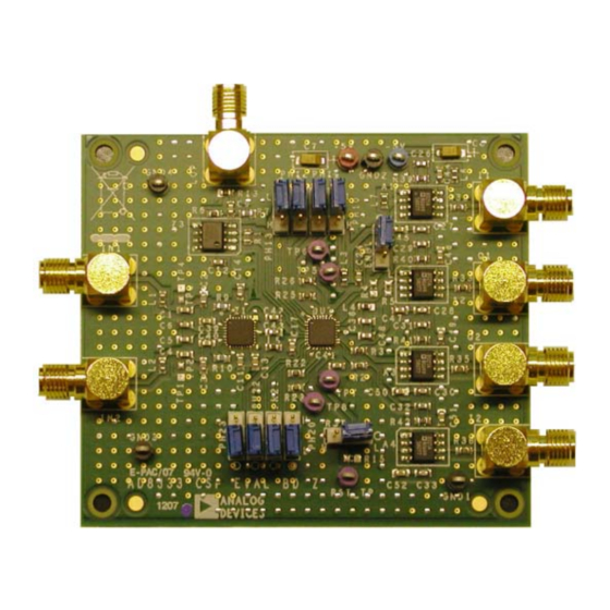
EVALUATION BOARD
Figure 1. Evaluation Board—Actual Size
One Technology Way, P.O. Box 9106, Norwood, MA 02062-9106, U.S.A.
Tel: 781.329.4700
Fax: 781.461.3113
Evaluation Board for the
AD8333 I/Q Demodulator
AD8333-EVALZ
©2006–2007 Analog Devices, Inc. All rights reserved.
www.analog.com
Advertisement
Table of Contents

Related Manuals for Analog Devices AD8333-EVALZ


Summary of Contents for Analog Devices AD8333-EVALZ
-
Page 1: Features
Devices for its use, nor for any infringements of patents or other rights of third parties that may result One Technology Way, P.O. Box 9106, Norwood, MA 02062-9106, U.S.A. from its use. Analog Devices reserves the right to change devices or specifications at any time Tel: 781.329.4700 www.analog.com... -
Page 2: Table Of Contents
AD8333-EVALZ TABLE OF CONTENTS Features ....................1 Measurement Setup...............4 Applications..................1 Evaluation Board Schematic and Artwork........5 General Description ................. 1 Board Layout..................7 Evaluation Board ................1 Ordering Information...............9 Revision History ................2 Bill of Materials................9 Introduction ..................3 Ordering Guide ................10 Features and Options .............. -
Page 3: Introduction
AD8333-EVALZ INTRODUCTION The AD8333-EVAL evaluation board provides a platform for Table 2. Phase Shift Select Codes test and evaluation of the AD8333 I/Q demodulator and phase Ф Shift PHx3 PHx2 PHx1 PHx0 shifter. The board is shipped fully assembled and tested, and the 0°... -
Page 4: Measurement Setup
AD8333-EVALZ MEASUREMENT SETUP Current Summing Figure 2 displays the connector and user-selectable jumper The output transimpedance amplifiers, A1 through A4, are locations. A typical board and test equipment setup is shown in configured as I-to-V converters to convert the output current of Figure 4. -
Page 5: Evaluation Board Schematic And Artwork
AD8333-EVALZ EVALUATION BOARD SCHEMATIC AND ARTWORK Figure 3. Evaluation Board Schematic Rev. B | Page 5 of 12... - Page 6 AD8333-EVALZ TOP: BOTTOM: SIGNAL GENERATOR FOR GENERATOR FOR RF INPUT INPUT TYPICAL SETTING: 20MHz TYPICAL SETTING: 5.01MHz SIGNAL 1V p-p POWER SUPPLY SYNCHRONIZE GENERATORS –5V POWER SPLITTER SIGNAL INPUT(S) Figure 4. Typical Board Test Connections (One Channel Shown) Rev. B | Page 6 of 12...
-
Page 7: Board Layout
AD8333-EVALZ BOARD LAYOUT The AD8333 evaluation board has four layers. The interconnecting circuitry is located on the outer layers with the inner layers dedicated as power and ground planes. Figure 5 through Figure 9 illustrate the copper patterns. Figure 7. Component Side Silkscreen Figure 5. - Page 8 AD8333-EVALZ Figure 9. Power Plane Rev. B | Page 8 of 12...
-
Page 9: Ordering Information
Description Reference Designator Mfg. Part Number Manufacturer AD8021ARZ A1 to A4 AD8021ARZ Analog Devices, Inc. Capacitor 0.1 μF, 16 V, 0603, X7R C0603C104K4RACTU KEMET Corporation C1, C4, C5, C6, C9, C11, C12, C13, C14, C17, C24, C36, C41, C42, C44, C45, C46, C47, C48, C49,... -
Page 10: Ordering Guide
AD8333-EVALZ ORDERING GUIDE ESD CAUTION Model Description AD8333-EVALZ Evaluation Board Z = RoHS Compliant Part. Rev. B | Page 10 of 12... - Page 11 AD8333-EVALZ NOTES Rev. B | Page 11 of 12...
- Page 12 AD8333-EVALZ NOTES ©2006–2007 Analog Devices, Inc. All rights reserved. Trademarks and registered trademarks are the property of their respective owners. EB05836-0-9/07(B) Rev. B | Page 12 of 12...
Need help?
Do you have a question about the AD8333-EVALZ and is the answer not in the manual?
Questions and answers