Advertisement
Quick Links
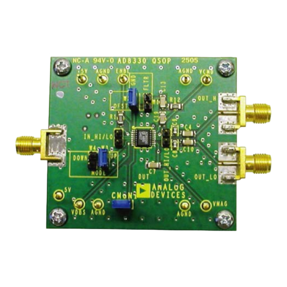
GENERAL DESCRIPTION
The EVAL-AD8330EB is an easy-to-use accessory that enables a
hands-on evaluation of the
AD8330
(VGA). It includes test pins for connections to all of the functional
device inputs. Figure 1 is a full size photograph of the board.
Figure 1. Photograph of the AD8330 Evaluation Board
IN
R5
49.9Ω
–5V
Rev. B
Information furnished by Analog Devices is believed to be accurate and reliable. However, no
responsibility is assumed by Analog Devices for its use, nor for any infringements of patents or other
rights of third parties that may result from its use. Specifications subject to change without notice. No
license is granted by implication or otherwise under any patent or patent rights of Analog Devices.
Trademarks and registered trademarks are the property of their respective owners.
variable gain amplifier
+5V
AGND
+5V
C1
+
10μF
10V
C14
C15
0.01μF
0.1μF
C3
0.1μF
3
AD8131
8
4
2
1
C18
5
0.1μF
6
R13
C5
24.9Ω
0.1μF
C16
0.01μF
C20
0.1μF
VDBS
0.1μF
AGND
C17
10μF
+
10V
AD8330 Evaluation Board
BASIC OPERATION
The input SMA connector IN is terminated with a 49.9 Ω
resistor (see Figure 2). For convenience, the board includes an
AD8131
high speed differential amplifier to convert a single-
ended signal source to the differential input of the AD8330. If
desired, the AD8131 can be removed and the AD8330 can be
driven at one of its inputs from a single-ended source.
The AD8330 output is observed at the SMA connectors OUT_HI
and OUT_LO or by using the 2-pin header OUT_HI/ OUT_LO
adjacent to the device.
The AD8330 requires only a +5 V power supply; however, because
of the AD8131 buffer bipolar power supply requirements, ±5 V
supplies are required to power the board. The current required
for the board is approximately 40 mA from the +5 V supply and
10 mA from the −5 V supply.
OPTIONS
Table 1 lists the jumpers on the board and their functions.
Consult the
functions.
C13
W1
1nF
FLTR
W2
OFST
1
OFST
VPOS
ENB
R1
0Ω
2
ENBL
CNTR
3
VPSI
C2
VPSO
0.1μF
4
OPHI
INHI
AD8330
IN_HI/LO
5
INLO
+5V
W3
UP
6
OPLO
MODE
W4
DOWN
7
VDBS
CMOP
C6
VMAG
CMGN1
8
COMM
CMGN
Figure 2. Schematic Diagram
One Technology Way, P.O. Box 9106, Norwood, MA 02062-9106, U.S.A.
Tel: 781.329.4700
Fax: 781.461.3113
EVAL-AD8330EB
AD8330
data sheet for further explanation of their
VCMD
AGND
R12
1kΩ
16
+5V
C12
0.1μF
15
C19
0.1μF
14
+5V
C11
C4
0.1μF
0.1μF
13
C9
12pF
OUT_HI/LO
C10
C8
0.1μF
12pF
12
11
10
VMAG
C7
9
0.1μF
AGND
©2006 Analog Devices, Inc. All rights reserved.
OUT_HI
OUT_LO
www.analog.com
Advertisement

Related Manuals for Analog Devices AD8330


Summary of Contents for Analog Devices AD8330
- Page 1 Information furnished by Analog Devices is believed to be accurate and reliable. However, no responsibility is assumed by Analog Devices for its use, nor for any infringements of patents or other One Technology Way, P.O. Box 9106, Norwood, MA 02062-9106, U.S.A.
- Page 2 EVAL-AD8330EB Table 1. Functions of Jumpers MEASUREMENT SETUP Name Function The basic board connections for a typical measurement are Connects a high-pass filter to the offset control loop shown in Figure 3. To minimize circuit-loading effects, a low pin. This jumper is normally not installed. capacitance FET probe is recommended for observing input or Disables the offset correction loop.
- Page 3 EVAL-AD8330EB Figure 4. Component-Side Silkscreen Figure 7. Wiring-Side Silkscreen Figure 5. Component-Side Wiring Figure 8. Wiring-Side Pattern Figure 6. Inner Layer 1 Figure 9. Inner Layer 2 Rev. B | Page 3 of 4...
- Page 4 ORDERING GUIDE Model Description AD8330-EVAL Evaluation Board ©2006 Analog Devices, Inc. All rights reserved. Trademarks and registered trademarks are the property of their respective owners. C03721-0-3/06(B) T T T Rev. B | Page 4 of 4...
Need help?
Do you have a question about the AD8330 and is the answer not in the manual?
Questions and answers