Analog Devices ADUC824 Reference Manual
Hide thumbs
Also See for ADUC824:
- Quick reference manual (2 pages) ,
- Get started manual (22 pages) ,
- User manual (16 pages)
Table of Contents
Advertisement
Quick Links
Download this manual
See also:
Quick Reference Manual
Advertisement
Table of Contents

Summary of Contents for Analog Devices ADUC824
- Page 1 C824 E VALUATION OARD EFERENCE UIDE ® ® C824 ICRO ONVERTER ™ ™ D UICK TART EVELOPMENT YSTEM...
-
Page 2: Version 1.0
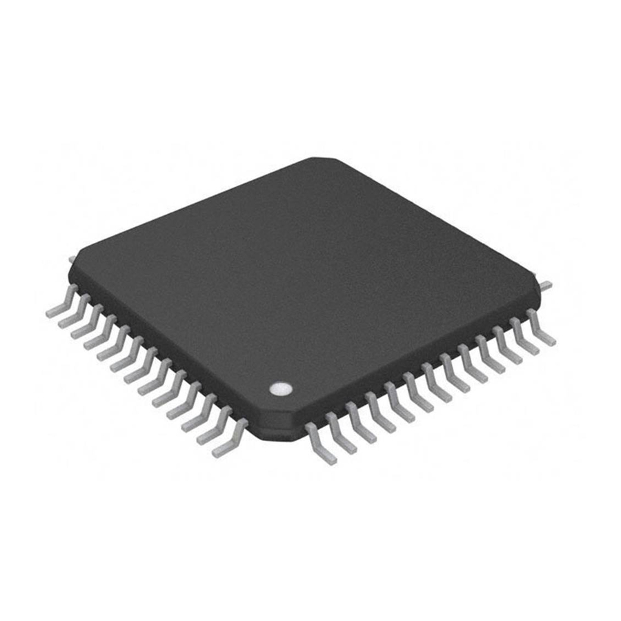
ADuC824 Evaluation Board Reference Guide ONTENTS Evaluation Board Reference Guide: 1) Evaluation Board Overview ......3 2) Evaluation Board Features . - Page 3 5V power supply is routed directly to the digital section and is filtered before being routed into the analog section of the board. 3. The ADuC824 can be socketed on the board using a QFP carrier adaptor and corresponding surface mount feet available from Ironwood Electronics The part numbers are CA-QFE52SB-L-Z-T-01 and SF-QFE52SB-L-01 respectively.
- Page 4 0.1uF at the digital supply pins. RS232 Interface: The ADuC824 (U1) TXD and RXD (pins 17 and 16 respectively) lines are connected via an RS232 transceiver (U2) to the external 9-way D-Type connector (J1). The transceiver generates the required level shifting to allow direct connection to a PC serial port.
-
Page 5: Evaluation Board Features
External Power on Reset Chip (ADM809) An external power on reset chip is used to drive the RESET pin on the ADuC824. Because we want a push button switch available to the user an active low Power on Reset chip (ADM809) is used with RESET output inverted (using a PNP BJT) before being connected to the RESET pin of the MicroConverter. -
Page 6: Version 1.0
(2) Evaluation Board Features Alternatively, if a push button switch is not required, the RESET output of an active high power on reset chip (e.g. ADM810) can be used to directly drive the RESET pin of the ADuC824. INT0 Push Buttons: Reset/INT0 A RESET push button is provided to allow the user to manually reset the part. -
Page 7: Link Options
Slide LK1 into the OFF position to disconnect P3.5 from the SPI SS line. LK2 (2x1) EA Pulldown Function: Allows the user to force the ADuC824 to execute the first 8kBytes of program memory from the internal or external program memory space. -
Page 8: Version 1.0
ADuC824 Evaluation Board Reference Guide (3) Link Options LK6 (3x1) DAC Output Link Function: The DAC output can be routed out on one of 2 pins. This link routes the selected DAC output pin through an external buffer to the external pin J2-13. -
Page 9: Version 1.0
Allows the External Data Memory to be used as both an External Program Memory and an External Data Memory. Slide LK13 into the ON position to connect the PSEN output from the ADuC824 (for use Use : with an external program memory) through an AND gate to the external data memory. This allows the external Data Memory to be used as both external program and data memory. -
Page 10: External Junctions (Connectors)
Table 1: Pin functions for Analog I/O connector J2 J3 (Timer/Strobe) The timer/strobe control signals on the ADuC824 are all brought out to a 10 way connection port just above the prototyping. The exact pinouts of the ports are shown in table 2 with reference to the connector shown in figure 3 below. -
Page 11: Of The Board
ADuC824 Evaluation Board Reference Guide (4) External Junctions (Connectors) Function Function T2EX DGND PSEN DVDD DGND Table 2: Timer/Strobe connector J3 J4/J5/J6 (Port0 / Port2 / Port 3) 3 parallel ports (Port0, Port2 and Port3) are brought out to the connectors J4, J5 and J6. The exact pinout of any of these connectors is shown below with reference to figure 3 above. -
Page 12: Rtd Temperature Demonstration Circuit
R11. This reference voltage is routed back to the Refin(+)/ Refin(-) inputs via LK7 and LK8. As described on page 35 of the ADuC824 datasheet the 0.1uF capacitors at REFIN+ and REFIN- will cause some dc error. Hence for optimum performance the two capacitors C13 and C29 should be removed while using the RTD demonstration. -
Page 13: Parts List
ADuC824 Evaluation Board Reference Guide (6) ADuC824 Evaluation Board Parts List (6) AD C824 E VALUATION OARD ARTS Component Part Description Order No Order From EVAL- ADuC824QS QuickStart PCB PCB-1 2 sided surface mount PCB PCB Stand-off Stand-off Stick on mounting feet... -
Page 14: Version 1.0
ADuC824 Evaluation Board Reference Guide (6) ADuC824 Evaluation Board Parts List R1, R2, R7-R10, R12, R14-R17 Surface Mount Resistor, 0603 Case 612-480 Farnell R3, R18 100K Surface Mount Resistor, 0603 Case 612-728 Farnell R4,R5 270R Surface Mount Resistor, 0603 Case...


Need help?
Do you have a question about the ADUC824 and is the answer not in the manual?
Questions and answers