
Subscribe to Our Youtube Channel
Related Manuals for Edge-Core AS7326-56X


Summary of Contents for Edge-Core AS7326-56X
- Page 1 EDGECORE Networks Corporation Edgecore AS7326-56X Programming Guide Revision 1.0 EDGECORE NETWORKS CORPORATION 2018...
-
Page 2: Revision History
Revision History Revision Date Author Description 9/15/2018 Jeff Catlin Initial Draft EDGECORE NETWORKS CORPORATION 2018... -
Page 3: Table Of Contents
Contents Revision History ............................... 2 Licenses ................................7 Introduction ............................9 1.1. Reference Documents ......................9 1.2. Acronyms and Terminology ....................9 Hardware Architecture ......................... 10 2.1. Overview ..........................10 2.2. Block Diagram ........................12 2.2.1. Clock Tree ..........................13 2.2.2. - Page 4 3.11.4. SMBUS ........................... 43 3.11.5. UART ............................43 3.11.6. USB ............................44 3.11.7. GPIO ............................44 3.12. CPLD (For CPU Board) ......................46 3.13. CPLD Architecture (For CPU Board) ..................47 3.13.1. Power Sequence ........................47 3.13.2. Reset ............................. 47 3.13.3.
- Page 5 4.7. SFP28 ............................. 67 4.8. SFP+ ............................67 Sub-system ............................68 5.1. Management PHY (BCM54616S) ..................68 5.2. Configurations of MGMT PHY (BCM54616S) ................ 68 5.3. POR of MGMT PHY (BCM54616S) ..................68 5.4. I2C ............................68 5.5. UART ............................72 5.6.
- Page 6 5.13.2. POR of IDT 8V89307 ......................177 5.14. PSU ............................178 5.14.1. Pinout ..........................178 5.14.2. Dimension ........................... 178 5.14.3. Efficiency ..........................179 5.14.4. Power Supply Management Controller (PSMC) ..............179 5.14.5. Power Supply Field Replacement Unit (FRU) ..............180 5.14.6.
-
Page 7: Licenses
Licenses All semiconductor devices that may be referred to in this specification, or required to manufacture products described in this specification, will be considered referenced only, and no intellectual property rights embodied in or covering such semiconductor devices shall be licensed as a result of this specification or such references. - Page 8 As of September 15, 2018, this specification is contributed under the OCP Contributor Licensing Agreement (OCP-CLA) by the following entities: Acton Technology Corporation, through its subsidiary Edgecore Networks Corporation Limitations of the OCP CLA license are noted below: No Limitations You can review the signed copies of the OCP-CLA for this specification on the OCP website.
-
Page 9: Introduction
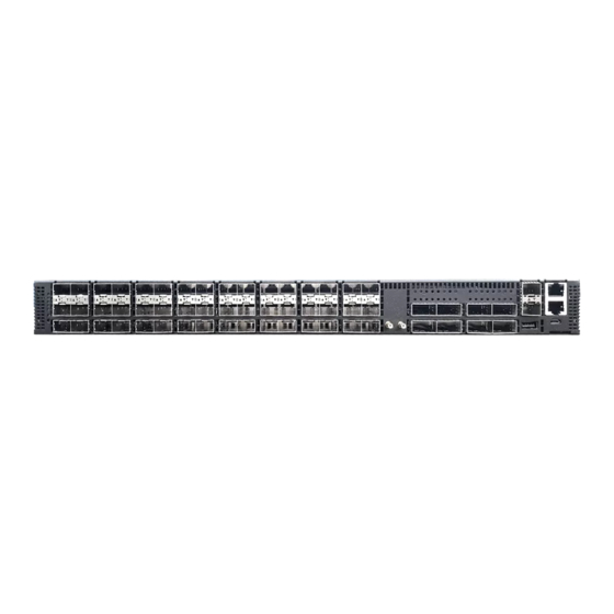
1. Introduction The Switch is a 1U high and 536mm deep chassis base on Broadcom Trident3 chipset. The physical layer will consist of 48x25G SFP28, 8x100G QSFP28 ports and 2x10G SFP+ ports. The chassis will have a nominal operating temperature range of 0 to +40 Degree C. The CPU board is for management of the switch board , the solution is Intel BroadWell- DE, that CPU board provide these interface: x4 PCIe2.0, SGMII, MDC/MDIO, USB2.0, and 2channel I2C connect to the switch board. -
Page 10: Hardware Architecture
This chapter describes the architecture of PCBA, cooling, power consumption, electrical, reset, clocks, Ethernet port mapping etc.. 2.1. Overview The AS7326-56X provides 48x25G SFP28, 8x100G QSFP28 and 2x10G SFP+ ports on the board and can support 1 x 1G ports for management and control. Table 1 System Overview AS7326-56X-0917-168ZZ CPU: Intel Broadwell-DE XeonD-1518 1.6G 4 Core... - Page 11 AS7326-56X-0917-168ZZ One type-A USB port at front panel, support USB 2.0 (480Mbps) CPLD CPLDs access by I2C and CPLDs code field upgraded by CPU GPIO RJ45 LED X’FMR One RJ45 with LED/one X’FMR embedded Broadcom Trident3 BCM56873, 1 pcs, 2000Gbs multi-layer Ethernet switch...
-
Page 12: Block Diagram
2.2. Block Diagram The AS7326-56X provides 48 x 25G ports, 8 x 100G ports and 2 x 10G ports on the board and can support 1 x 1G port for management and control. It is formed by BCM56873, a 20 Falconcore with max. -
Page 13: Clock Tree
10GeB SPI flash 74AVCH4T245 TTL1T45 25MHz 32.768Khz 25MHz DDR4 SO-DIMM 0 DDR-CH0 SATA M.2 connector (option) PCA9617 DDR_I2C SATA mSATA BDX-DE DDR4 SO-DIMM 1 DDR-CH1 eUSB Debug usb System SPI flash (Pri) PCIE2_6 SML0_1 System SPI flash (Sec) SVID VCCIN=0X00 Level LPC header VCCSUSCUS=0X01... -
Page 14: Power Tree
25MHz Clock XTAL M6163LF OCXO 156.25MHz To 56873 (FC7_8_REFCLK) Differential 156.25MHz OCXO12.8MHz 156.25MHz Differential To 56873 (FC23_24_REFCLK) 25MHz 156.25MHz L1_RCVRD_CLK 156.25MHz RMS Jitter Max Requirement: IP_UART0_SIN OSCI To 56873 (MC_REFCLK) Single-End IDT8V89307_IN1p/n Differential Core_50M: 10ps From CPU Single-End IN1_P/N L1_RCVRD_CLK_VALID 1PPS_GPIO2 Reference_156.25M: 0.3ps GATE... - Page 15 Power tree To Fan Board FAN *(5+1) (12V/1.7A *6) To CPU Board 12V max 70.8A For BMC CPLD1 12V/6A For BMC_MGMT PHY Power sharing Power module BMC_VDD1P2/0.2A AP7362 For BMC MGMT PHY Vstb_3V3/2A (1.2A LDO) TPS54329DDAR (3A) For PWR_Monitor/ IR_Control Vstb CPLD_VDD1P8/0.1A AP7362...
-
Page 16: Reset Tree
VIN12 1.7V 1.3V 3V3_A 1.05V 1V8_A 1.2V TPS54426 TPS54426 TPS74701DRCR 5V_STBY@6A 1.7V@2A 1.3@0.5A 1.5V_PCH P3V3 1.8V BDXDE 1.7V_EN P3V3_PCH 1.3V_EN 1.2V TPS54426 2.5V_EN DDR4-SODIMM 2.5V@2.88A 0.6V TPS74701DRCR 1.5V_PCH@0.3A 2.5V 1.5V_PCH_EN TPS54426 5V_STBY SATA connector P3V3@2.5A P3V3_PCH P3V3 CPLD TPS54426 5V_STBY 3V3_A@2.5A AX6631SA P3V3... - Page 17 Reset 120Pins PCA9548 PCA9548 PCA9548 PCA9548 BTB Connector PCA9548_10~16_RESET_N PCA9548 PCA9548 PCA9548 CPLD1 0x60 PCA9548 PCA9548_00~02_RESET_N PCA9548 PCA9548 CPU_JTAG_RST Reserved MAC_RESET_N MAC BCM56873 RESET_MAC WAN PLL IDT8V89307_RST IDT8V89307 RESET_SYS_CPLD P49~P56_RESET_N QSFP28 *8 MANU_RST MGMT_PHY_RST_N MGMT BCM4616S USB_RESET_N USB HUB PCIE_PERST_L MAC BCM56873 Delay 120ms...
-
Page 18: Front/Rear Placement
Level CPLD_CPU_PCH_PLTRST_N BTB 120pin RESET_CPU_N shift RTCRST_N PCH_PLTRST_N PLTRST_N I210 U6 PCH_RSMRST_N RSMRST_N PE_RST_N Level CPLD_BDX_CPU_RSMRST RSMRST_CPU_N BDXDE shift PCIE_RST_N RESET_SYS_CPLD PCH_SYSRESET_N SYS_RESET_N PSHBTN_SYS_RESET_N CPLD Manu_RST PSHBTN_SYS_RESET_N PCH_PWRBTN_N PWRBTN_N PCA9548_RST_N PCA9548 SYS_PWRBTN_N DDR4- sodimm P1014_RST 2.3. Front/Rear Placement Figure 9 System Front/Rear Placement 3. -
Page 19: Configurations Of Cpu
Figure 10 MAC Sub-System Topology PCIE2 x2 BCM5720 NCSI BMC Module SGMII/Serdes BCM54616S Main Board 3.1. Configurations of CPU ➢ 2 DDR channels support DDR4 ECC and non-ECC UDIMM, SODIMM, RDIMM ➢ Memory speed : DDR4 1600, 1867, 2133, 2400 MT/s ➢... -
Page 20: Por Of Cpu
for I2C devices Supports intel Virtualization Technology for Directed I/O (Intel VT-d) Supports intel Trusted Execution Technology (Intel TXT) Integrated clock controller Low Pin Count (LPC) interface Firmware Hub (FWH) interface support Serial Peripheral Interface (SPI) support ... - Page 21 No power sequencing between Vccin and VCCD is required. ➢ Phase 1: PCU bring-up Phase 1a: Activity Leading to PCU Start-up Assertion of PWRGOOD_CPU (the trigger to move from the end Phase 0 to thestart of Phase 1a). ...
- Page 22 Pcode performs boot mode processing based on straps. Set the advertised firmware, IO, and Intel TXT agent bits appropriately. Pcode services DMI2 handshake protocol. If DMI2 links are used in DMI2 mode, pcode checks if the links have trained to L0. If it's the legacy socket, and if DMI2 links does not reach L0 within 3-4 ms, pcode executes error flow.
-
Page 23: Interface
Figure 12 Power Sequencing Diagram S5 to S0 3.2. 1G Interface The 1G interface could support SGMII or SERDES link, currently configuration is set to SERDES EDGECORE NETWORKS CORPORATION 2018... -
Page 24: Software Configurations Of Cpu
mode to connect BCM54616S in order to support PXE boot function. Figure 13 Management port function 3.3. Software Configurations of CPU Figure 14 GPIO CPU_TDO BDX_CPLD_JTAG_TDO GPIO10 THERMTRIP CPU_THERMALTRIP CPLD Level CPU_PROCHOT shift PROCHOT_N LM75 GPIO14 buffer CPU_TCK GPIO18 CPU_TMS CPU_TDI GPIO9 GPIO25... - Page 25 Figure 15 power sequence flow chat State S5 PF_painc =0 G3_panic =0 Led1=0 Led2=1 PCH_SLP_S4_N =1 & PCH_SYS_PWORK= PCH_PWRBTN_N=1 & s0_flag=1 State S0 PF_painc =0 G3_panic =0 Led1=1 Led2=1 S0_flag=1 State G3 PF_painc =1 G3_panic =1 PCH_SYS_PWORK= Holdrails =0 Led1=1 Led2=0 S0_flag=0 PCH_SLP_S3_N==1...
- Page 26 Table 3 GPIO Pin name GPIO_USE_SEL GPIO_IO_SEL function 1: GPIO 1: input 0: Native 0: output GPIO0 BMBUSY# GPIO1 TACH1. GPIO2 PIRQE# GPIO3 PIRQF#. GPIO4 PIRQG# GPIO5 PIRQH# GPIO6 GPIO7 GPIO8 PCH_XDP_NCLK1 GPIO9 XDP_NOA5_PCH/ BDX_CPLD_JTAG_TDI GPIO10 XDP_NOA6_PCH/ BDX_CPLD_JTAG_TDO GPIO11 SMBALERT# GPIO12 LAN_PHY_PWR_CTRL GPIO14...
- Page 27 GPIO23 GPIO24 USB1_VBUS GPIO25 1PPS_CPU GPIO26 SYS_CPLD_INT_CPU GPIO27 SOC_FPGA_DIN GPIO28 SOC_FPGA_DOUT GPIO29 IP_UART0_SOUT GPIO30 IP_UART0_SIN GPIO31 SMB_PWR_ALERT GPIO32 GPIO33 4.7K TO GND GPIO35 FM_NMI_EVENT_PCH_N/ FM_NMI_EVENT_CPLD_N GPIO36 ADR_STATUS_RD GPIO37 ADR_STATUS_CLR GPIO38 SLOAD GPIO39 SDATAOUT0 GPIO40 OC1# GPIO41 XDP_NOA2_PCH/ CPLD_CONFIG_CLK GPIO42 XDP_NOA3_PCH/ CPLD_CONFIG_DATA GPIO43 XDP_NOA4_PCH_R...
- Page 28 GPIO53 1k pull to gnd GPIO54 GPIO55 FM_BIOS_RCRV_BOOT_N GPIO57 FM_ME_RCRV_N GPIO58 SML1_CLK GPIO59 XDP_NOA0_PCH/ USB1_PWRFAULT GPIO60 SML0ALERT# GPIO61 GPIO62 PCH_SUSCLK_33K GPIO65 GPIO67 GPIO68 GPIO69 GPIO70 GPIO71 GPIO72 1K pull to 3.3V GPIO74 SML1ALERT#/TEMP_ALERT#. GPIO75 SML1DATA Table 4 PCH Strap definitions Strap pin description value...
- Page 29 in conjunction with Boot BIOS Destination Selection 0 strap. SATA3GP /GPIO37 0 = Disable Intel ME Crypto Transport Layer Security (TLS) cipher suite (no confidentiality). 1 = Enable Intel ME Crypto Transport Layer Security (TLS) cipher suite (with confidentiality). MFG_MODE_STRAP 0 = Enable security measures defined in the Flash Descriptor.
- Page 30 address lines (A16, A17, A18, A19, or A20) as selected in Top-Swap Block size soft strap (handled through FITc. 1 = Disable “Top Swap” mode. GPIO8 This pin must not be driven low until after rising edge of RSMRST_N. GPIO44 This pin must not be driven low until after rising edge of RSMRST_N.
-
Page 31: Memory Mapping
RSVD12_AJ67 This pin should have a 5.1K ohm pull down to GND. RSVD11_AG67 This pin should have a 5.1K ohm pull down to GND. RSVD10_AN78 This pin should have a 5.1K ohm pull down to GND. RSVD09_AC64 This pin should have a 5.1K ohm pull down to GND. - Page 32 Bus0:Device31:Function6 Thermal subsystem Bus0:Device29:Function0 USB EHCI controller#1 Bus0:Device28:Function0 PCI-e port1 Bus0:Device28:Function1 PCI-e port2 Bus0:Device28:Function2 PCI-e port3 Bus0:Device28:Function3 PCI-e port4 Bus0:Device28:Function4 PCI-e port5 Bus0:Device28:Function5 PCI-e port6 Bus0:Device28:Function6 PCI-e port7 Bus0:Device28:Function7 PCI-e port8 Bus0:Device25:Function0 Gigabit Ethernet controller Bus0:Device22:Function0 Intel management engine interface#1 Bus0:Device22:Function1 Intel management engine interface#2 Bus0:Device22:Function2...
- Page 33 reserved NMI and RTC controller RTC controller RTC controller RTC controller NMI and RTC controller RTC controller RTC controller RTC controller NMI and RTC controller RTC controller RTC controller RTC controller NMI and RTC controller RTC controller RTC controller DMA controller, LPC, PCI or PCIe DMA controller, LPC, PCI or PCIe 81h-83h DMA controller...
- Page 34 IDE bus master Anywhere in 64KB I/O space 1. 16 or 32 1. SATA host controller #1, #2 2. 16 2. IDE-R Native IDE command Anywhere in 64KB I/O space 1. SATA host controller #1, #2 2. IDE-R Native IDE control Anywhere in 64KB I/O space 1.
- Page 35 FF88 0000h- FF8F FFFFh FFD0 0000h-FFD7 FFFFh LPC or SPI (or PCI) Bit 10 in BIOS decode enable register is set FF90 0000h- FF97 FFFFh FFD8 0000h-FFDF FFFFh LPC or SPI (or PCI) Bit 11 in BIOS decode enable register is set FF98 0000h- FF9F FFFFh FFE0 0000h-FFE7 FFFFh LPC or SPI (or PCI)
-
Page 36: Flash
anywhere in 64-bit address range 4 KB anywhere in 64-bit address Thermal Reporting Enable using standard PCI mechanism (D31:F6 range TBAR/ TBARH) 4 KB anywhere in 64-bit address Thermal Reporting Enable using standard PCI mechanism (D31:F6 range TBARB/TBARBH) 16 Bytes anywhere in 64-bit Intel®... -
Page 37: Ram
BDX_SPI_MUX_SEL SPI_CS_SELECT CPLD BIOS_SPI_KGI_N BIOS_SPI2_CS_switch 128Mb BIOS_SPI_CS1 BIOS_SPI2_CS BIOS_SPI_CLK_DI_DO Clk/di/do SPI_CS1# BIOS_SPI_CI_N 128Mb BMC_SPI_CS0 Clk/di/do 2A/3A/4A BIOS_SPI1_CS SPI_CLK_MOSI_MISO SPI_MUX_OE_N BDXDE CONN2 SF100_IO3 Jumper BDX_SPI_MUX_SEL BMC_CLK_DI_DO CI_KGI_SELECT BMC_SPI_CS_N CONN3 CONN14 Dediprog BMC_SPI_OUT_SEL LAN_FLASH_CK BIOS_SPI_CLK_DI_DO LAN_FLASH_DO Level LAN_FLASH_CS_N 32Mb shift LAN_FLASH_DI NVM_SI OE# S U43 Function MUX Function... -
Page 38: Pcie
DDR0_CLK[0:1] DDR0_MA[16:0] DDR0_BA[1:0] DDR0_BG[1:0] DDR0_ACT_N DDR0_PAR DDR4 DDR0_CS_N[1:0] Sodimm-0 DDR0_CKE[1:0] DDR0_ODT[1:0] DDR0_DQ[63:0] DDR0_DQS[8:0] DDR0_ECC[7:0] BDXDE DDR0_ALERT_N DDR3_4_STRAP VCCIOIN DDR1_CLK[0:1] DDR1_MA[16:0] DDR1_BA[1:0] DDR1_BG[1:0] DDR1_ACT_N DDR1_PAR DDR4 DDR1_CS_N[1:0] Sodimm-1 DDR1_CKE[1:0] DDR1_ODT[1:0] DDR1_DQ[63:0] DDR1_DQS[8:0] DDR1_ECC[7:0] DDR1_ALERT_N 3.7. PCIe The CPU board has to provide the x4 PCIE Gen3 and x1 PCIE Gen2 to main board. The x4 PCIE GEN3 is used to connect the NP8365 for control path, the PCIE GEN2 x1 is sued to communicate the OOB. -
Page 39: I2C/Smbus Architecture
120pins BTB connector CPU_PEX_PCIE[B:A]_TX_[1:0]_N PE1_TX_DN[3:0] CPU_PEX_PCIE[B:A]_TX_[1:0]_P PE1_TX_DP[3:0] PE1_RX_DN[3:0] CPU_PEX_PCIE[B:A]_RX_[1:0]_N PE1_RX_DP[3:0] CPU_PEX_PCIE[B:A]_RX_[1:0]_P PCIE2_TX_DN[6] PCIE_OOB_TX_N PCIE_OOB_TX_P PCIE2_TX_DP[6] PCIE2_RX_DN[6] PCIE_OOB_RX_N PCIE2_RX_DP[6] PCIE_OOB_RX_P BDXDE PCIE2_TX_DN[5] PCIE2_TX_DP[5] PCIE2_RX_DN[5] PCIE2_RX_DP[5] PCIE2_TX_DN[0:1] PE_RN PE_RP PCIE2_TX_DP[0:1] BCM5720 PCIE2_RX_DN[0:1] PE_TN PE_TP PCIE2_RX_DP[0:1] 3.8. I2C/SMBus Architecture The SMbus from Broadwell-DE can access the CPU board and main board device via SMBUS0. The multiplexers(MUX) are used to prevent multi-master issues on the SMBUS. - Page 40 SODIMM1 DDR_I2C Level shift CONN7 0x50 EEPROM SODIMM2 SMBCLK CONN8 0X56 SMBDATA 0x52 U40/U41 CPU XDP CONN4 IR3570 PCH XDP I2C:0x4 CONN11 I2C3 PMBUS:0x40 CPLD I2C_Multiplexer_Select 0x65 IR3584 I2C:0x2 PMBUS:0x26/0x28 BDXDE BMM CONN LM75 LM75 0X4B 120pin PCA9548 I2C0 connector I2C1 0X77 I2C2...
-
Page 41: Sata
IR3584 (PMBUS-Loop1) 0x26 IR3584 (PMBus-Loop2) 0x28 IR3570 (I2C) IR3570 0x42 (PMBus Loop1) PCA9548 0X77 For main board 3.9. SATA The CPU board supports 2 SATA SSD devices via SATA 3.0 interface. SATA 3.0 CH0 support mSATA SSD module. SATA 3.0 CH1 support m.2 SSD module. The following table shows the mSATA and m.2 SSD module dimension and size. -
Page 42: Base-Kr
3.10. 10G-Base-KR The 10GBE interface of the multiplexer switches Broadwell-DE CPU uses 10G-KR to communicate with the MAC BCM56873 to support additional high speed datalink between CPU and MAC. Figure 21 10GBase-KR Connection Broadwell-DE (CPU Board) 10G-KR x2 DS100MB203 BCM56873 10G-KR x2 (Main Board) (Main Board) -
Page 43: Lpc
STBY_3.3V@2.7A STBY_5V@2A TPS54426 Front-Panel UART Main Board STBY_3.3V@0.5A UART0_RX UART0_TX STBY_3.3V@1.2A UART_SEL UART0 UART0_RX STBY_5V@0.1A UART0 Level shift UART0_TX SMB0 UART1 BDXDE UART1 I2C3 SML(0/1) I2C MUX USB2.0 BDXDE PCIE CLK PCIE GEN2 x1 BMC_HW_PRESENT BDX_PECI_PCH MB_PWR_STATUS BDX_INTRUDER_N PS_PWR_OK CPLD_CPU_PROCHOT_N CPLD_CPU_THERMTRIP_N BCM5720 Fault_LED_OUT... -
Page 44: Usb
If BMC want to send UART message to CPU via UART0 of CPU, “BMC_UART0_DIR_SEL” would be driven to “0” from “1”. Figure 23 UART connection UART0 Level shift 120pin BTB connector BDXDE UART1 Level shift Table 11 CONN18 PIN ASSIGNMENT Pin Number Description 3.11.6. - Page 45 BDX_PECI_PCH PECI_CPU detect CPLD_interrupt CPLD interrupt to CPU All the power in the PS_PWROK signal chassis would be PS_PWROK All_power_reset from CPLD reset when this pin is “0” All the power in the INTRUDER# BDX_INTRUDER_N chassis would be off All_power_off function when this pin is “0”...
-
Page 46: Cpld (For Cpu Board)
this action When the NMI event has been sent NMI_BTN_IN_BMC_N to CPU, BMC need to know this event 3.12. CPLD (For CPU Board) The aim of the CPLD on the BDXDE CPU Board in the ES7654NT chassis is major for power sequence, reset system, system interrupt, and BMC module function support. -
Page 47: Cpld Architecture (For Cpu Board)
3.13. CPLD Architecture (For CPU Board) 3.13.1. Power Sequence The most important function of the CPLD is to control the whole board power sequence based on the power sequence requirement of Intel Broadwell-DE. CPLD would base on the power good signals from the VRs on the board and then drives the enable signals to enable the VRs. -
Page 48: Interrupt
Due to match old platform, some net name have not been changed and not match their function, like below: “CPU_JTAG_RST” is used to announce MB that BMC want to light the ID led. “MAC_INT_L” is used to announce MB that BMC want to light off the DIAG led. “USB1_VBUS”... -
Page 49: Thermal
Figure 27 CPLD SDATA Diagram SDATA SOC_FPGA_CLK SOC_FPGA_DIN SOC_FPGA_DOUT BDX_SATA1_ACTIVITY_LED1 BDX_SATA1_ACTIVITY_LED2 SDATA BDX_SCLOCK Decorder BDX_SDATAOUT0 BDX_SDATAOUT1 BDX_SLOAD 3.13.7. Thermal The thermal block is used to monitor the thermal event driven from CPU by “CPLD_CPU_PROCHOT_N” / “CPLD_DDR01_MEMHOT”, “VR_PVCCIN_VRHOT_N” / ” VR_P1V05_PCH_VRHOT_N” / ” P1V2_VDDQ_IRQ_VRHOT_N” from VRs, and “CPLD_DDR_EVENT_N” from DDR memory, then use “CPLD_PCHHOT_N”... -
Page 50: Cpld Register (For Cpu Board)
3.14. CPLD Register (For CPU Board) Table 13 CPLD I/O Register Summary Address Register Default value 0x00 Board Info Read Only 0x02 0x01 CPLD version Read Only 0x07 0x02 BIOS boot flash select 0x03 Reset - System 0x04 Reset - device 0x05 Interrupt Event Read Only... -
Page 51: Offset 0X04 Reset - Device (Read& Write)
0: system would enter sleep mode system reset 1: system is work at S0 state 0: system would be reset System Power Off 1: system is work at S0 state 0: all power on the board would be powered off except standby voltage. -
Page 52: Offset 0X07 Thermal Status (Read& Write)
0: Indicates THERMTRIP was signaled due to an internal error with the integrated voltage regulator rather than an over temperature condition. CPU ERROR 2 1: CPU is placed in normal operation state. 0: Fatal error (system reset likely required to recover) CPU ERROR 1 1: CPU is placed in normal operation state. - Page 53 Light: P3V3 power fail OFF: P3V3 power ok LED2 P1V7 (VCCSCFUSESUS) power LED Color: Red Light: P1V7 power fail OFF: P1V7 power ok LED3 P1V3 (VCCKRHV) power LED Color: Red Light: P1V3 power fail OFF: P1V3 power ok LED4 P1V05 power LED Color: Red Light: P1V05 power fail OFF: P1V05 power ok...
-
Page 54: Gpio
Color: Green Bright: M.2 DATA transmission OFF: no M.2 data transmission LED15 No function. LED17 PCH_SYS_PWROK LED Color: Green Light: pch system power ok OFF: pch system power fail LED18 MAC link LED Color: Green Light: MAC link up OFF: MAC link down LED19 System State LED Color: Bi, O , R... - Page 55 BDX_CPLD_JTAG_TDI BDX_CPLD_JTAG_MUX_ENABLE BDX_CPLD_JTAG_TDO JTAG_TDI JTAG_TDO TDI_MOSI GPIO9 GPIO10 GPIO61 TDO_MISO THERMTRIP CPU_THERMALTRIP CPLD Level CPU_PROCHOT shift PROCHOT_N LM75 CPLD_JTAG_MUX_ENABLE GPIO8 JTAG_TCK GPIO14 CPU_TCK GPIO18 JTAG_TMS CPU_TMS GPIO9 GPIO25 1PPS_CPU GPIO26 SYS_CPLD_INT_CPU BDXDE GPIO44 MAC_INT_L CPLD23_INT_CPU GPIO45 CPLD CPU_JTAG_RST GPIO46 USB1_PWRFAULT GPIO59 USB1_VBUS GPIO24...
- Page 56 GPIO2 GPIO3 GPIO4 CPU to PCH Throttle event interrupt GPIO5 GPIO6 JTAG enable, enable JTAG multiplexer to update CPLD code from CPU. 1: enable the JTAG multiplexer 0: disable the JTAG multiplexer GPIO7 GPIO8 JTAG Multiplexer select, which select the JTAG signals from CPU would go to CPLD or main board 1: to CPLD (default) 0: to Main board...
- Page 57 GPIO18 XDP_NOA14_PCH/ BDX_CPLD_JTAG_TMS GPIO19 BI-DIR XDP_NOA9_PCH GPIO20 FM_SMI_ACTIVE_PCH_N/ FM_SMI_ACTIVE_CPLD_N GPIO21 BI-DIR XDP_NOA8_PCH GPIO22 SCLOCK GPIO23 GPIO24 GPIO25 1PPS_CPU (no use) GPIO26 SYS_CPLD_INT_CPU GPIO27 SOC_FPGA_DIN GPIO28 SOC_FPGA_DOUT GPIO29 IP_UART0_SOUT(no use) GPIO30 IP_UART0_SIN(no use) GPIO31 SMB_PWR_ALERT GPIO32 GPIO33 GPIO35 FM_NMI_EVENT_PCH_N/ FM_NMI_EVENT_CPLD_N GPIO36 ADR_STATUS_RD GPIO37 ADR_STATUS_CLR...
-
Page 58: Sub-System Of Mac (Bcm56873)
GPIO46 CPU_JTAG_RST(no use) GPIO48 SDATAOUT1 GPIO49 FM_CPU_PROCHOT_PCH_N/ FM_PROCHOT_N GPIO50 GPIO51 4.7k pull to 3.3V GPIO52 CPU_SV GPIO53 1k pull to gnd GPIO54 GPIO55 FM_BIOS_RCRV_BOOT_N GPIO57 FM_ME_RCRV_N GPIO58 SML1_CLK GPIO59 XDP_NOA0_PCH GPIO60 SML0ALERT# GPIO61 GPIO62 SUSCLK_33K GPIO65 GPIO67 GPIO68 CPLD interrupt GPIO69 GPIO70 GPIO71... -
Page 59: Configurations Of Mac (Bcm56873)
4.1. Configurations of MAC (BCM56873) Table 16 MAC Configurations Table Pin Number Pin Name Function Description BG24 BOOT_DEV[2:0] Selects the boot flow for mHost0 (the first internal ARM R5): 3’b000: Load all necessary code from QSPI flash attached to IP_QSPI interface and begin execution. (others): Reserved Note: These signals have no effect if MHOST0_BOOT_DEV is pulled low... -
Page 60: Por Of Mac (Bcm56873)
BA24 PCIE_FORCE_GENTYPE[1:0] Selects the maximum operating rate of the PCI Express interface: BB24 2’b00: Interface can operate at PCI Express Gen1, Gen2, or Gen3 speeds 2’b01: Interface can operate at PCI Express Gen1 speed 2’b10: Interface can operate at PCI Express Gen1, Gen2 speeds (others): Reserved Note: When the PCI Express interface is configured to support Gen3 speeds, it is a requirement that the MHOST0_BOOT_DEV... -
Page 61: Port Mapping
4.3. Port Mapping Figure 31 Physical Port mapping EDGECORE NETWORKS CORPORATION 2018... - Page 62 Table 17 MAC Mapping Table Mac(BCM56873) Connector SFP28 Port Number FalconCore Connector TX polarity RX polarity (front-end) TX polarity RX polarity Location (TD) (RD) FC0_TD2[P/N] FC0_RD2[P/N] CONN20A TD[+/-]#1T RD[+/-]#1T Port1 FC0_TD1[P/N] FC0_RD3[P/N] CONN20A TD[+/-]#1L RD[+/-]#1L Port2 FC0_TD3[P/N] FC0_RD1[P/N] T_TD[+/-] T_RD[+/-] Port3 FC1_TD3[N/P] FC1_RD3[P/N]...
- Page 63 FC1_TD2[N/P] FC1_RD2[N/P] CONN20B TD[+/-]#2L RD[+/-]#2L Port5 FC0_TD0[N/P] FC0_RD0[P/N] T_TD[+/-] T_RD[+/-] Port6 FC1_TD0[N/P] FC1_RD0[P/N] CONN21A TD[+/-]#1T RD[+/-]#1T Port7 FC3_TD3[N/P] FC3_RD3[N/P] CONN21A TD[+/-]#1L RD[+/-]#1L Port8 FC1_TD1[P/N] FC1_RD1[P/N] T_TD[+/-] T_RD[+/-] Port9 FC3_TD1[P/N] FC3_RD1[N/P] CONN21B TD[+/-]#2T RD[+/-]#2T Port10 FC3_TD0[P/N] FC3_RD2[N/P] CONN21B TD[+/-]#2L RD[+/-]#2L Port11 FC3_TD2[P/N] FC3_RD0[N/P] T_TD[+/-]...
- Page 64 FC16_TD1[P/N] FC16_RD1[P/N] CONN26B TD[+/-]#2L RD[+/-]#2L Port41 FC15 FC15_TD0[P/N] FC15_RD0[P/N] T_TD[+/-] T_RD[+/-] Port42 FC16 FC16_TD3[N/P] FC16_RD3[N/P] CONN27A TD[+/-]#1T RD[+/-]#1T Port43 FC17 FC17_TD0[N/P] FC17_RD0[N/P] CONN27A TD[+/-]#1L RD[+/-]#1L Port44 FC16 FC16_TD2[N/P] FC16_RD2[P/N] T_TD[+/-] T_RD[+/-] Port45 FC17_TD2[P/N] FC17_RD2[N/P] CONN27B TD[+/-]#2T RD[+/-]#2T Port46 FC17 FC17_TD3[P/N] FC17_RD1[N/P] CONN27B TD[+/-]#2L...
-
Page 65: 25G/40G/100G Interface
MC_TD2[P/N] MC_RD2[P/N] TD[+/-]#1L RD[+/-]#1L Port58 4.4. 10G/25G/40G/100G Interface AS7326-56X is phy-less system, BCM56873 connects with SFP28、QSFP28 and SFP+ directly and CPU control transceiver’s I2C and status via CPLD. Figure 32 10G/40G/100G Interface Connection 120 Pins BTB Connector 10G-KR x2 BCM56873... - Page 66 ➢ IP_LED_clk/data1 provides port status for SFP+ ports 57-58. Port status information includes link status, transmit and receive activity, and speed settings The interface to the LED status indicators is implemented through a serial protocol carried out on two pins: LED_CLK and LED_DATA. If there are n LED status lights, it takes clock cycles to shift the data out of the LED interface.
-
Page 67: Qsfp28
100G 4 x 25G 4 x 10G 2 x 50G Link-up/ Activity Toggle Activity Type LED bit stream(b0 … b13) SFP+ QSFP 00-000-000-000-000 00-111-111-111-111 N/A(off) N/A (off) 00-001-001-001-001 Amber/Yellow Purple 00-101-101-101-101 Green Amber/Yellow 10-001-001-001-001 N/A(off) Blue 100G 10-101-101-101-101 N/A(off) Green xx-xxx-xxx-xxx-xxx N/A(off) Green... -
Page 68: Sub-System
5. Sub-system 5.1. Management PHY (BCM54616S) The management port support 10/ 100/ 1000M Ethernet speed. 5.2. Configurations of MGMT PHY (BCM54616S) Table 20 MGMT PHY Configurations Table Pin Number Pin Name Function Description LED1 LED1 High >> Copper AN enable LED2 LED2 High >>... - Page 69 Figure 34 Switch board I2C Connection SW Board FAN Board 8V89307 0x54 0x70 120Pins 8T49N240 0x7C BTB Connector FAN_SCL_1/SDA 0x62 I2C_0_SCL/SDA_CPLD2 CPLD 2 PCA9548 PSU2 PSU2 SMBUS:0x5B 0x27 I2C_0_SCL/SDA EEPROM:0x53 IOEXP 50/48 EEPROM_SCL/SDA 0x57 EEPROM LM75BD_SCLK/SDA IR3595A 0x10 PSU1 PSU1 SMBUS:0x59 0x66 EEPROM:0x51...
- Page 70 LM75BD_CPU switch_CH7 IR3595A 0x10 SMBUS:0x59 switch_CH0 PSU1 EEPROM:0x51 switch_CH1 CPLD1 0x60 switch_CH2 0x64 CPLD3 switch_CH3 0x12 IR3595B I2C 0 switch_CH4 0x25 P1014 I2C switch (71) SFP+:0x50 SFP+ switch_CH5 MUX:0x58 SFP+:0x51 SFP+ switch_CH6 Retimer:0x18 Retimer switch_CH7 0x72 I2C switch (72) switch_CH0 0x50, 0x51 QSFP28 PORT 49 switch_CH1...
- Page 71 switch_CH5 0x50, 0x51 SFP28 PORT 7 switch_CH6 0x50, 0x51 SFP28 PORT 5 switch_CH7 0x50, 0x51 SFP28 PORT 9 switch_CH0 0x50, 0x51 SFP28 PORT 10 switch_CH1 0x50, 0x51 SFP28 PORT 8 switch_CH2 0x50, 0x51 SFP28 PORT 12 I2C 1 switch_CH3 0x50, 0x51 SFP28 PORT 11 I2C switch (72) switch_CH4...
-
Page 72: Uart
switch_CH6 0x50, 0x51 SFP28 PORT 38 switch_CH7 0x50, 0x51 SFP28 PORT 40 switch_CH0 0x50, 0x51 SFP28 PORT 41 switch_CH1 0x50, 0x51 SFP28 PORT 42 switch_CH2 0x50, 0x51 SFP28 PORT 45 I2C 1 switch_CH3 0x50, 0x51 SFP28 PORT 43 I2C switch (76) switch_CH4 0x50, 0x51 SFP28 PORT 44... -
Page 73: Usb
RJ45_DSR RJ45_CTS 5.6. USB There are three USB 2.0 interfaces in the project. The USB-0 via the 120pins BTB connector to switch board for chassis external type A USB connector, USB-1 is for debug function and USB-2 connect to eUSB module for internal USB access. The mapping table and connection are as below. -
Page 74: Jtag
Shutdown_wake 5.8. JTAG AS7326-56X had only done the JTAG download chain for three CPLD with JTAG interface, it make the CPLD programing more quickly. The TCK and TMS pass to all devices by buffer. TDI and TDI are connecting directly. -
Page 75: Led Indicator
CPLD1_TCK CPU_TCK CPLD2_TCK MAC_TCK PHY_TCK CONN Buffer JTAG Tree CPLD1_TMS CPU_TMS CPLD2_TMS MAC_TMS CPU_TDI PHY_TMS JTAG_TCK JTAG_TMS JTAG CONN PHY_TCK FAN_TCK PHY_TMS FAN_TMS FAN CPLD MultiPlexer JTAG_TDI FAN_TDI CPLD1_TDO FAN_TDO S = 0 CPLD1, CPLD2, CPLD3 chain S = 0 output =>BU_CPLD2_TDO 1 Fan CPLD CPLD3_TDI 1 output =>BU_PHY_TDI... -
Page 76: Port Led
(Power Supply Power supply not present. Status) Green System FAN operating normally. Fan tray present buy system FAN is fault. System OFF Green System self-diagnostic test successfully completed. Diag System self-diagnostic test has detected a fault. (Fan, (Diagnostic) thermal or any interface fault.) System OFF Flashing by remote management command. - Page 77 There is no link on the port. QSFP28 port has a valid link at 25G via On/Flashing break out cable. The LED on 100G QSFP Yellow end is also present OFF. Flashing indicates activity. (With Breakout cable) There is no link on the port. QSFP28 port has a valid link at 10G via On/Flashing break out cable.
-
Page 78: Management Port Led
Yellow Flashing indicates activity. There is no link on the port. Figure 42 SFP+ Port LED Table 26 SFP+ Port LED Definition Color Mode On/Flashing SFP+ port has a valid link at 10G. Green Flashing indicates activity. SFP+ Port LED SFP+ port has a valid link at 1G. -
Page 79: Button
5.11. Thermal system 5.11.1. Temperature sensor There are five temperature sensors in AS7326-56X system, and the locations are shown in the picture below. CPU can access the sensor via I2C interface, and the sensor has the interrupt signal connect with CPLD for over-temp event application. - Page 80 Figure 46 CPU board - Temp sensor location Bottom EDGECORE NETWORKS CORPORATION 2018...
-
Page 81: Fan Controller System
5.11.2. Fan controller system The Fan board has a CPLD to do the fan controller function. The CPLD on the Fan board can control the Fan’s PWM signal for adjust Fan speed and count the Fan’s Tach signal for Fan speed reporting. CPU can read the thermal sensor to get thermal information, and then adjust Fan speed to reduce system’s thermal. - Page 82 Figure 48 Fan Speed information Figure 49 Fan failed information EDGECORE NETWORKS CORPORATION 2018...
-
Page 83: Cpld
The system only can provide 3.3V PWM signal. The min of Vh of fan need be low than 3.3V. 5.12. CPLD AS7326-56X has three CPLD devices for decoding, Fan module status, reset system, power module status and System interrupt. I2C address info:... - Page 84 *CPLD3:0x64 *Fan_CPLD:0x66 Figure 51 CPLD Block Diagram CPLD Block diagram 8V89307 PCA9548 0x54 I2C SWITCH 8T49N240 0x7C 0x70 Front port LED (P1~33) CPLD 2 PCA9548 I2C SWITCH 0x62 Board version/ information Front port Interrupt 0x71 CPLD 1 Front port reset I2C device 0x60 Front port LED...
- Page 85 0x29 Port10 0x19 Port47 0x2A Port11 0x30 Port49 LED0 0x2B Port12 0x31 Port49 LED1 0x2C Port13 0x32 Port49 LED2 0x2D Port14 0x33 Port49 LED3 0x2E Port15 0x34 Port50 LED0 0x2F Port16 0x35 Port50 LED1 0x30 Port17 0x36 Port50 LED2 0x31 Port18 0x37 Port50 LED3...
-
Page 86: Cpld1 Pin-Out List
5.12.1. CPLD1 pin-out list Table 30 CPLD1 Pin-out List Net name IN/ OUT 1PPS_CLK CPLD3_INT RESET_SYS_CPLD RESET_MAC Manu_RST CPU_THERMALTRIP CPLD1_25MHz Board_ID1 USB1_PWRFAULT SFP+_MOD_ABS_P29 FAN_G SFP+_RXLOS_P36 M12 SFP+_DIS_P36 PCA9548_14_RESET_N P53_RESET_N BU_SEL_2 PCA9548_13_RESET_N PCIE_PERST_L P55_MODPRSNT_N SFP+_RXLOS_P30 P54_MODPRSNT_N IP_TS_GPIO1_2 Reserved PCB_Version2 SYS_CPLD_INT_CPU I2C_0_SDA_CPLD1 IN/OUT M15 UART1_RX SFP+_MOD_ABS_P37... - Page 87 SFP+_DIS_P29 PS1_PDB_ALERT RX_LOSS_FX1 TX_FAULT_FX0 PS2_EEPROM_WP Reserved CPU_JTAG_RST POWER_RST CPLD2_INT Board_ID2 FAN_INT_L P49_MODPRSNT_N P50_MODPRSNT_N USB1_VBUS PRESENT_FX0 M16 1PPS_CPU PS2_12V_PG PS1_AC-OK Reserved USB_UART_RX TX_FAULT_FX1 SFP+_MOD_ABS_P38 SFP+_MOD_ABS_P39 SFP+_FLT_P34 FAN_SDA_2 IN/OUT SFP+_FLT_P38 SFP+_MOD_ABS_P33 EE_WP FAN_SCL_2 SFP+_RXLOS_P33 SFP+_FLT_P47 shutdown_wake SFP+_FLT_P37 FAN_B SFP+_DIS_P40 SFP+_DIS_P42 SFP+_DIS_P47 EDGECORE NETWORKS CORPORATION 2018...
- Page 88 SFP+_DIS_P48 SFP+_FLT_P35 SFP+_FLT_P39 PS1_PRESENT SFP+_RXLOS_P39 SFP+_MOD_ABS_P46 SFP+_DIS_P46 PSU1_G SFP+_RXLOS_P46 PSU1_R PSU1_B SFP+_DIS_P38 1PPS_GPIO2 M11 SFP+_FLT_P36 USB_UART_SUSPEND_L Reserved PCIE_WAKE_L Reserved PS1_ON PCIE_INTR_L PCA9548_02_RESET_N PCA9548_12_RESET_N SFP+_RXLOS_P48 SFP+_MOD_ABS_P48 IP_BS0_CLK_2 Reserved CPLD_USB_VBUS_DET PCA9548_00_RESET_N M10 SFP+_MOD_ABS_P40 SFP+_FLT_P45 SFP+_FLT_P43 CPLD23_INT_CPU SFP+_MOD_ABS_P44 SFP+_DIS_P45 MAC_INT_L Reserved PCA9548_10_RESET_N PCA9548_11_RESET_N CPLD_RST EDGECORE NETWORKS CORPORATION 2018...
- Page 89 PCA9548_01_RESET_N N/A(CPLD_IP_BS0) PCA9548_15_RESET_N SFP+_FLT_P41 PCA9548_16_RESET_N LM75BD0_INT PSU2_G IDT8V89307_RST SFP+_RXLOS_P41 DIAG_G FAN_R Reset_button_RST SFP+_FLT_P46 IP_CPLD_BS0_HB Reserved SFP+_MOD_ABS_P34 PSU2_B PSU2_R SFP+_MOD_ABS_P47 SFP+_RXLOS_P43 SFP+_MOD_ABS_P45 SFP+_FLT_P44 SFP+_MOD_ABS_P36 SFP+_RXLOS_P42 SFP+_DIS_P43 LOC_B SFP+_DIS_P39 SFP+_FLT_P33 SFP+_FLT_P40 SFP+_RXLOS_P34 SFP+_DIS_P33 SFP+_RXLOS_P29 SFP+_DIS_P44 SFP+_MOD_ABS_P43 SFP+_MOD_ABS_P35 SFP+_RXLOS_P35 EDGECORE NETWORKS CORPORATION 2018...
- Page 90 L1_RCVRD_CLK_VALID SFP+_RXLOS_P44 P52_INT SFP+_RXLOS_P45 PS2_AC-OK Reserved DIAG_B SFP+_MOD_ABS_P42 PS2_PDB_ALERT BU_SEL_1 LOC_R System_B Reserved P50_INT RS232_UART_RX UCD9090_ALERT_L Reserved I2C_0_SCL_CPLD1 PS2_ON P51_INT PCB_Version1 LM75BD1_INT P56_MODPRSNT_N P54_RESET_N SFP+_RXLOS_P37 P55_INT P53_MODPRSNT_N P54_INT P51_RESET_N P56_RESET_N LM75BD_SDA IN/OUT DIAG_R System_R Reserved System_G Reserved LOC_G LM75BD2_INT P49_INT PS1_AC_ALERT EDGECORE NETWORKS CORPORATION 2018...
- Page 91 PS2_AC_ALERT P51_MODPRSNT_N PS1_EEPROM_WP Reserved SFP+_FLT_P48 SFP+_RXLOS_P47 LM75BD_SCLK P53_INT TX_DIS_FX1 RX_LOSS_FX0 CPU_PROCHOT P56_INT P55_RESET_N SFP+_RXLOS_P40 P50_RESET_N PS2_PRESENT IDT8V89307_INT_REQ P49_RESET_N USB_PWRON_N IP_CPLD_BS0_TC Reserved Fan_idle Reserved L1_RCVRD_CLK_VALID_BKUP SFP+_DIS_P41 PRESENT_FX1 TX_DIS_FX0 USB_RESET_N USB_PWRFLT_N SFP+_FLT_P42 P52_RESET_N FAN_SDA_1 IN/OUT FAN_SCL_1 PS1_12V_PG SFP+_DIS_P34 M13 SFP+_DIS_P30 M14 SFP+_FLT_P30 MGMT_PHY_RST_N EDGECORE NETWORKS CORPORATION 2018...
-
Page 92: Cpld 1 Register
INT_MGMT_PHY_N SFP+_MOD_ABS_P41 SFP+_DIS_P35 SFP+_DIS_P37 SFP+_RXLOS_P38 5.12.2. CPLD 1 Register Table 31 CPLD1 Register Table Address Register Default value 0x00 Board Info Read Only 0x0E 0x01 PCB version Read Only 0x00 0x02 Power module status-1 Read Only 0x3C 0x03 Power module status-2 Read&... - Page 93 Offset 0x00 Board Info (Read Only) Name Reset Value Description Reserved 3:2 PCB_ID[1:0] 00 for 01 for 10 for 11 for AS7326-56X 1:0 PCB_version[1:0] 00 for R0A 01 for R0B 10 for R0C 11 for R01 5.12.2.2. Offset 0x01 CPLD version (Read Only) Name...
- Page 94 0: Enable power supply (Default) PS[1:2]_ON 1: Shutdown power supply 5.12.2.5. Offset 0x04 System Reset-1 (Read& Write) Name Reset Value Description Reset* P56 QSFP28 1: transceiver is placed in normal operation state. (Default) (P56_RESET_N) 0: transceiver is placed in reset state. Reset* P55 QSFP28 1: transceiver is placed in normal operation state.
- Page 95 5 Reset* PCA9548_ 1: PCA9548 is placed in normal operation state. (Default) I2C_1; 0x75 (PCA9548_15_RESET_N) 0: PCA9548 is placed in reset state. 4 Reset* PCA9548_ 1: PCA9548 is placed in normal operation state. (Default) I2C_1; 0x74 (PCA9548_14_RESET_N) 0: PCA9548 is placed in reset state. 3 Reset* PCA9548_ 1: PCA9548 is placed in normal operation state.
- Page 96 0: CPU_JTAG_RST is placed in reset state. RESET_SYS_CPLD 1: RESET_SYS_CPLD is placed in normal operation state. 0: RESET_SYS_CPLD is placed in reset state. 1: Non-push the push button of front panel RESET_BUTTON_RST 0: Push the push button of front panel POWER_RST POWER_RST is placed in normal operation state.
- Page 97 Reserve INTB*IDT8V89307 1: No interrupt (IDT8V89307_INT_REQ) 0: There is INTR from IDT8V89307 INTB*FAN 1: No interrupt (FAN_INT_L) 0: There is INTR from FAN INTB*CPLD3 1: No interrupt (CPLD3_INT) 0: There is INTR from CPLD2 INTB*CPLD2 1: No interrupt (CPLD2_INT) 0: There is INTR from CPLD3 INTB* LM75_3 1:No interrupt (LM75BD2_INT)
- Page 98 MASK* P52 QSFP28 1: CPLD blocks incoming the interrupt 0: CPLD passes the interrupt to CPU (Default) MASK* P51 QSFP28 1: CPLD blocks incoming the interrupt 0: CPLD passes the interrupt to CPU (Default) MASK* P50 QSFP28 1: CPLD blocks incoming the interrupt 0: CPLD passes the interrupt to CPU (Default) MASK* P49 QSFP28...
- Page 99 Present* P38 SFP28 1: No transceiver (SFP+_MOD_ABS_P39) 0: transceiver had plugged Present* P37 SFP28 1: No transceiver (SFP+_MOD_ABS_P38) 0: transceiver had plugged Present* P36 SFP28 1: No transceiver (SFP+_MOD_ABS_P35) 0: transceiver had plugged Present* P35 SFP28 1: No transceiver (SFP+_MOD_ABS_P33) 0: transceiver had plugged Present* P34 SFP28 1: No transceiver...
- Page 100 5.12.2.19. Offset 0x12 Module Present -3 (Read Only) Name Reset Value Description Reserve Present* P58 SFP+ 1: No transceiver (PRESENT_FX1) 0: transceiver had plugged Present* P57 SFP+ 1: No transceiver (PRESENT_FX0) 0: transceiver had plugged Present* P48 SFP28 1: No transceiver (SFP+_MOD_ABS_P46) 0: transceiver had plugged Present* P47 SFP28...
- Page 101 (SFP+_DIS_P38) 0: transceiver is under transmit enable (Default) Disable* P36 SFP28 1: transceiver is under transmit disable (SFP+_DIS_P35) 0: transceiver is under transmit enable (Default) Disable* P35 SFP28 1: transceiver is under transmit disable (SFP+_DIS_P33) 0: transceiver is under transmit enable (Default) Disable* P34 SFP28 1: transceiver is under transmit disable...
- Page 102 Disable* P58 SFP+ 1: transceiver is under transmit disable (TX_DIS_FX1) 0: transceiver is under transmit enable (Default) Disable* P57 SFP+ 1: transceiver is under transmit disable (TX_DIS_FX0) 0: transceiver is under transmit enable (Default) Disable* P48 SFP28 1: transceiver is under transmit disable (SFP+_DIS_P46) 0: transceiver is under transmit enable (Default)
- Page 103 RX_LOSS* P43 SFP28 1: transceiver Loss (SFP+_RXLOS_P44) 0: transceiver is working well RX_LOSS* P42 SFP28 1: transceiver Loss (SFP+_RXLOS_P37) 0: transceiver is working well RX_LOSS* P41 SFP28 1: transceiver Loss (SFP+_RXLOS_P42) 0: transceiver is working well RX_LOSS* P40 SFP28 1: transceiver Loss (SFP+_RXLOS_P41) 0: transceiver is working well RX_LOSS* P39 SFP28...
- Page 104 0: transceiver is working well Fault* P32 SFP28 1: transceiver Fault (SFP+_FLT_P36) 0: transceiver is working well Fault* P31 SFP28 1: transceiver Fault (SFP+_FLT_P29) 0: transceiver is working well 5.12.2.28. Offset 0x1B Module Fault-2 (Read Only) Name Reset Value Description Fault* P46 SFP28 1: transceiver Fault (SFP+_FLT_P47)
- Page 105 5.12.2.30. Offset 0x20 Recovery_CLKvalid&1PPS Mask (Read& Write) Name R/W Reset Value Description 7 IP_CPLD_BS0_TC Reserve 6 IP_CPLD_BS0_HB Reserve 5 IP_BS0_CLK_2 Reserve 4 IP_TS_GPIO1_2 Reserve L1_RCVRD_CLK_VALID_backup 1:L1_RCVRD_CLK backup is VALID 0:L1_RCVRD_CLK backup is not VALID 2 L1_RCVRD_CLK_VALID 1:L1_RCVRD_CLK is VALID 0:L1_RCVRD_CLK is not VALID 1 Mask *1PPS_GPIO2 1: CPLD passes 1pps signal to1pps_GPIO2 (Default)
- Page 106 status signals (Default) 0: PSU2 status by S/W. PSU2_Blinking_B 1: PSU2_B Blinking ON 0: PSU2_B Blinking OFF (Default) PSU2_Blinking_G 1: PSU2_G Blinking ON 0: PSU2_G Blinking OFF (Default) PSU2_Blinking_R 1: PSU2_R Blinking ON 0: PSU2_R Blinking OFF (Default) PSU2_B 1: PSU2_B LED OFF (Default) 0: PSU2_B LED ON PSU2_G...
- Page 107 DIAG_Blinking_R 1: DIAG_R Blinking ON 0: DIAG_R Blinking OFF (Default) DIAG_B 1: DIAG_B LED OFF (Default) 0: DIAG_B LED ON DIAG_G 1: DIAG_G LED OFF (Default) 0: DIAG_G LED ON DIAG_R 1: DIAG_R LED OFF (Default) 0: DIAG_R LED ON 5.12.2.35.
-
Page 108: Cpld2 Pin-Out List
5.12.2.37. Offset 0x27 USB (Read & Write) Name Reset Value Description Reserved USB_PWRON_N 1: USB enable (Default) 0: USB disable USB1_VBUS 1: USB enable 0: USB disable 1: No interrupt (Default) USB1_PWRFAULT 0: There is INTR to CPU USB_PWRFLT_L 1: No interrupt 0: There is INTR from USB 5.12.2.38. - Page 109 Net name IN/ OUT P3_Lane2_LED_B P46_Lane1_LED_R P2_Lane1_LED_R P2_Lane1_LED_B SFP+_RXLOS_P2 SFP+_MOD_ABS_P2 P3_Lane2_LED_R P2_Lane1_LED_G SFP+_DIS_P3 SFP+_FLT_P3 SFP+_DIS_P31 P4_Lane3_LED_B P4_Lane3_LED_G P8_Lane3_LED_B SFP+_RXLOS_P3 SFP+_FLT_P31 IP_LED_DATA2 P4_Lane3_LED_R P7_Lane2_LED_G SFP+_MOD_ABS_P3 SFP+_FLT_P2 SFP+_MOD_ABS_P28 SFP+_MOD_ABS_P21 SFP+_RXLOS_P21 P7_Lane2_LED_B P8_Lane3_LED_G SFP+_RXLOS_P4 SFP+_MOD_ABS_P4 SFP+_DIS_P25 SFP+_FLT_P24 P1_Lane0_LED_B P8_Lane3_LED_R SFP+_FLT_P4 SFP+_DIS_P4 SFP+_RXLOS_P27 P1_Lane0_LED_R EDGECORE NETWORKS CORPORATION 2018...
- Page 110 P7_Lane2_LED_R SFP+_RXLOS_P7 SFP+_MOD_ABS_P7 SFP+_DIS_P2 SFP+_DIS_P8 P1_Lane0_LED_G SFP+_FLT_P8 SFP+_RXLOS_P1 SFP+_MOD_ABS_P32 SFP+_FLT_P25 P5_Lane0_LED_B P12_Lane3_LED_B SFP+_MOD_ABS_P1 SFP+_DIS_P1 SFP+_FLT_P28 SFP+_DIS_P18 P5_Lane0_LED_G P12_Lane3_LED_G SFP+_FLT_P1 SFP+_RXLOS_P8 SFP+_DIS_P28 P5_Lane0_LED_R P12_Lane3_LED_R SFP+_MOD_ABS_P8 SFP+_FLT_P7 P6_Lane1_LED_B P6_Lane1_LED_G SFP+_DIS_P7 P6_Lane1_LED_R SFP+_MOD_ABS_P12 IP_LED_CLK1 P23_Lane2_LED_B P22_Lane1_LED_G IP_LED_DATA1 SFP+_RXLOS_P25 P22_Lane1_LED_B P18_Lane1_LED_G EDGECORE NETWORKS CORPORATION 2018...
- Page 111 P29_Lane0_LED_G P32_Lane3_LED_R P36_Lane3_LED_R P36_Lane3_LED_B P32_Lane3_LED_B P28_Lane3_LED_R P31_Lane2_LED_B P3_Lane2_LED_G P31_Lane2_LED_G P22_Lane1_LED_R P23_Lane2_LED_G P21_Lane0_LED_R P21_Lane0_LED_G P21_Lane0_LED_B P18_Lane1_LED_R P35_Lane2_LED_R P25_Lane0_LED_B P25_Lane0_LED_G P25_Lane0_LED_R P31_Lane2_LED_R P36_Lane3_LED_G P32_Lane3_LED_G P28_Lane3_LED_B P19_Lane2_LED_G P27_Lane2_LED_R P27_Lane2_LED_B P30_Lane1_LED_B P30_Lane1_LED_R P46_Lane1_LED_G P43_Lane2_LED_R P43_Lane2_LED_B P40_Lane3_LED_R P40_Lane3_LED_B P29_Lane0_LED_R P20_Lane3_LED_B P28_Lane3_LED_G EDGECORE NETWORKS CORPORATION 2018...
- Page 112 P27_Lane2_LED_G P23_Lane2_LED_R P30_Lane1_LED_G P46_Lane1_LED_B SFP+_RXLOS_P28 P43_Lane2_LED_G P40_Lane3_LED_G P29_Lane0_LED_B P19_Lane2_LED_B SFP+_FLT_P18 SFP+_FLT_P22 SFP+_RXLOS_P26 IP_LED_CLK2 IP_LED_DATA0 IP_LED_CLK0 SFP+_MOD_ABS_P20 SFP+_FLT_P27 SFP+_DIS_P27 SFP+_RXLOS_P23 SFP+_MOD_ABS_P23 IP_LED_CLK4 IP_LED_DATA4 P26_Lane1_LED_G P17_Lane0_LED_R P26_Lane1_LED_B P26_Lane1_LED_R P24_Lane3_LED_G P24_Lane3_LED_R SFP+_DIS_P23 SFP+_FLT_P23 SFP+_RXLOS_P20 P17_Lane0_LED_G P24_Lane3_LED_B SFP+_RXLOS_P22 SFP+_FLT_P20 SFP+_RXLOS_P32 SFP+_MOD_ABS_P25 EDGECORE NETWORKS CORPORATION 2018...
- Page 113 SFP+_DIS_P32 P17_Lane0_LED_B SFP+_MOD_ABS_P26 SFP+_MOD_ABS_P22 SFP+_RXLOS_P19 SFP+_DIS_P20 SFP+_FLT_P32 SFP+_MOD_ABS_P31 SFP+_DIS_P21 P18_Lane1_LED_B SFP+_MOD_ABS_P19 P35_Lane2_LED_B SFP+_DIS_P14 SFP+_MOD_ABS_P15 SFP+_FLT_P14 P35_Lane2_LED_G SFP+_MOD_ABS_P18 SFP+_RXLOS_P18 SFP+_FLT_P16 SFP+_RXLOS_P15 P37_Lane0_LED_B P37_Lane0_LED_G SFP+_DIS_P22 SFP+_RXLOS_P17 SFP+_FLT_P17 SFP+_MOD_ABS_P16 SFP+_DIS_P16 P37_Lane0_LED_R EDGECORE NETWORKS CORPORATION 2018...
- Page 114 P13_Lane0_LED_G SFP+_MOD_ABS_P13 SFP+_MOD_ABS_P24 SFP+_MOD_ABS_P11 SFP+_RXLOS_P16 P13_Lane0_LED_R P13_Lane0_LED_B SFP+_FLT_P15 SFP+_FLT_P11 P19_Lane2_LED_R P20_Lane3_LED_G P20_Lane3_LED_R SFP+_DIS_P11 SFP+_RXLOS_P31 SFP+_DIS_P26 SFP+_FLT_P26 I2C_0_SDA_CPLD2 IN/OUT SFP+_MOD_ABS_P27 SFP+_RXLOS_P13 SFP+_DIS_P19 IP_LED_CLK3 IP_LED_DATA3 SFP+_DIS_P10 SFP+_FLT_P10 SFP+_FLT_P19 SFP+_MOD_ABS_P14 SFP+_DIS_P24 CPLD_RST CPLD2_INT SFP+_RXLOS_P24 SFP+_RXLOS_P9 SFP+_RXLOS_P10 SFP+_DIS_P9 SFP+_FLT_P9 SFP+_DIS_P5 SFP+_FLT_P5 EDGECORE NETWORKS CORPORATION 2018...
- Page 115 SFP+_MOD_ABS_P17 SFP+_DIS_P17 SFP+_MOD_ABS_P9 SFP+_RXLOS_P12 SFP+_RXLOS_P6 SFP+_DIS_P6 SFP+_MOD_ABS_P6 SFP+_RXLOS_P5 SFP+_DIS_P12 P10_Lane1_LED_B P14_Lane1_LED_R P14_Lane1_LED_B SFP+_MOD_ABS_P10 I2C_0_SCL_CPLD2 SFP+_RXLOS_P14 SFP+_DIS_P15 SFP+_RXLOS_P11 P16_Lane3_LED_G P9_Lane0_LED_B P9_Lane0_LED_G P9_Lane0_LED_R P11_Lane2_LED_G SFP+_FLT_P6 SFP+_MOD_ABS_P5 SFP+_FLT_P12 P14_Lane1_LED_G P15_Lane2_LED_B P15_Lane2_LED_G P15_Lane2_LED_R P16_Lane3_LED_B P16_Lane3_LED_R EDGECORE NETWORKS CORPORATION 2018...
-
Page 116: Cpld 2 Register
P10_Lane1_LED_G P10_Lane1_LED_R P11_Lane2_LED_B P11_Lane2_LED_R SFP+_FLT_P13 SFP+_DIS_P13 CPLD2_25MHz SFP+_FLT_P21 5.12.4. CPLD 2 Register Table 33 CPLD2 Register Table Address Register Default value 0x02 0x01 CPLD version Read Only 0x01 CPLD2 interrupt 0x02 Read &Write 0xff Module Fault-1 0x03 Read Only 0xff Module Fault-2 0x04 Read Only... - Page 117 0x07 SFP28 RGB LED -2 0x21 Read &Write 0x07 SFP28 RGB LED -3 0x22 Read &Write 0x07 SFP28 RGB LED -4 0x23 Read &Write 0x07 SFP28 RGB LED -5 0x24 Read &Write 0x07 SFP28 RGB LED -6 0x25 Read &Write 0x07 SFP28 RGB LED -7 0x26...
- Page 118 0x07 SFP28 RGB LED -38 0x45 Read &Write 5.12.4.1. Offset 0x01 CPLD version (Read Only) Name Reset Value Description 0x03 CPLD_ver[7:0] CPLD version 5.12.4.2. Offset 0x02 CPLD interrupt(Read & Write) Name Reset Value Description Reserved CPLD2_INT 1:No interrupt(Default) 0: Sent interrupt request to CPLD1 5.12.4.3.
- Page 119 Fault* P15 SFP28 1: transceiver Fault(Default) (SFP+_FLT_P16) 0: transceiver is working well Fault* P14 SFP28 1: transceiver Fault(Default) (SFP+_FLT_P14) 0: transceiver is working well Fault* P13 SFP28 1: transceiver Fault(Default) (SFP+_FLT_P15) 0: transceiver is working well Fault* P12 SFP28 1: transceiver Fault(Default) (SFP+_FLT_P11) 0: transceiver is working well...
- Page 120 Reserved Fault* P30 SFP28 1: transceiver Fault(Default) (SFP+_FLT_P25) 0: transceiver is working well Fault* P29 SFP28 1: transceiver Fault(Default) (SFP+_FLT_P31) 0: transceiver is working well Fault* P28 SFP28 1: transceiver Fault(Default) (SFP+_FLT_P32) 0: transceiver is working well Fault* P27 SFP28 1: transceiver Fault(Default) (SFP+_FLT_P28)
- Page 121 0: transceiver is under transmit enable (Default) Disable* P15 SFP28 1: transceiver is under transmit disable (SFP+_DIS_P16) 0: transceiver is under transmit enable (Default) Disable* P14 SFP28 1: transceiver is under transmit disable (SFP+_DIS_P14) 0: transceiver is under transmit enable (Default) Disable* P13 SFP28 1: transceiver is under transmit disable...
- Page 122 5.12.4.10. Offset 0x0A Module Disable-4 (Read& Write) Name Reset Value Description Reserved 5 Disable* P30 SFP28 1: transceiver is under transmit disable (SFP+_DIS_P25) 0: transceiver is under transmit enable (Default) 4 Disable* P29 SFP28 1: transceiver is under transmit disable (SFP+_DIS_P31) 0: transceiver is under transmit enable (Default)
- Page 123 5.12.4.12. Offset 0x0C Module RX_LOSS-2 (Read Only) Name Reset Value Description RX_LOSS* P16 SFP28 1: transceiver Loss (Default) (SFP+_RXLOS_P20) 0: transceiver is working well RX_LOSS* P15 SFP28 1: transceiver Loss (Default) (SFP+_RXLOS_P16) 0: transceiver is working well RX_LOSS* P14 SFP28 1: transceiver Loss (Default) (SFP+_RXLOS_P14)
- Page 124 (SFP+_RXLOS_P19) 0: transceiver is working well 5.12.4.14. Offset 0x0E Module RX_LOSS-4 (Read Only) Name Reset Value Description Reserved RX_LOSS* P30 SFP28 1: transceiver Loss (Default) (SFP+_RXLOS_P25) 0: transceiver is working well RX_LOSS* P29 SFP28 1: transceiver Loss (Default) (SFP+_RXLOS_P31) 0: transceiver is working well RX_LOSS* P28 SFP28 1: transceiver Loss (Default)
- Page 125 5.12.4.16. Offset 0x10 Module Present-2 (Read Only) Name Reset Value Description Present* P16 SFP28 1: No transceiver(Default) (SFP+_MOD_ABS_P20) 0: transceiver had plugged Present* P15 SFP28 1: No transceiver(Default) (SFP+_MOD_ABS_P16) 0: transceiver had plugged Present* P14 SFP28 1: No transceiver(Default) (SFP+_MOD_ABS_P14) 0: transceiver had plugged Present* P13 SFP28 1: No...
- Page 126 Present* P17 SFP28 1: No transceiver(Default) (SFP+_MOD_ABS_P19) 0: transceiver had plugged 5.12.4.18. Offset 0x12 Module Present-4 (Read Only) Name Reset Value Description 7:6 Reserved Present* P30 SFP28 1: No transceiver(Default) (SFP+_MOD_ABS_P25) 0: transceiver had plugged Present* P29 SFP28 1: No transceiver(Default) (SFP+_MOD_ABS_P31) 0: transceiver had plugged...
- Page 127 0: Port2_B Active OFF (Default) Port2_Active_G 1: Port2_G Active ON (P2_Lane1_LED_G) 0: Port2_G Active OFF (Default) Port2_Active_R 1: Port2_R Active ON (P2_Lane1_LED_R) 0: Port2_R Active OFF (Default) Port2_B 1: Port2_B LED OFF (Default) (P2_Lane1_LED_B) 0: Port2_B LED ON Port2_G 1: Port2_G LED OFF (Default) (P2_Lane1_LED_G) 0: Port2_G LED ON...
- Page 128 Port4_R 1: Port4_R LED OFF (Default) (P8_Lane3_LED_R) 0: Port4_R LED ON 5.12.4.23. Offset 0x24 SFP28 RGB LED -5 (Read& Write) Name Reset Value Description Reserve Port5_Active_B 1: Port5_B Active ON (P7_Lane2_LED_B) 0: Port5_B Active OFF (Default) Port5_Active_G 1: Port5_G Active ON (P7_Lane2_LED_G) 0: Port5_G Active OFF (Default)
- Page 129 Port7_Active_R 1: Port7_R Active ON (P5_Lane0_LED_R) 0: Port7_R Active OFF (Default) Port7_B 1: Port7_B LED OFF (Default) (P5_Lane0_LED_B) 0: Port7_B LED ON Port7_G 1: Port7_G LED OFF (Default) (P5_Lane0_LED_G) 0: Port7_G LED ON Port7_R 1: Port7_R LED OFF (Default) (P5_Lane0_LED_R) 0: Port7_R LED ON 5.12.4.26.
- Page 130 5.12.4.28. Offset 0x29 SFP28 RGB LED -10 (Read& Write) Name Reset Value Description Reserve Port10_Active_B 1: Port10_B Active ON (P10_Lane1_LED_B) 0: Port10_B Active OFF (Default) Port10_Active_G 1: Port10_G Active ON (P10_Lane1_LED_G) 0: Port10_G Active OFF (Default) Port10_Active_R 1: Port10_R Active ON (P10_Lane1_LED_R) 0: Port10_R Active OFF (Default)
- Page 131 (P11_Lane2_LED_B) 0: Port12_B LED ON Port12_G 1: Port12_G LED OFF (Default) (P11_Lane2_LED_G) 0: Port12_G LED ON Port12_R 1: Port12_R LED OFF (Default) (P11_Lane2_LED_R) 0: Port12_R LED ON 5.12.4.31. Offset 0x2C SFP28 RGB LED -13 (Read& Write) Name Reset Value Description Reserve Port13_Active_B 1: Port13_B Active ON...
- Page 132 (P16_Lane3_LED_B) 0: Port15_B Active OFF (Default) Port15_Active_G 1: Port15_G Active ON (P16_Lane3_LED_G) 0: Port15_G Active OFF (Default) Port15_Active_R 1: Port15_R Active ON (P16_Lane3_LED_R) 0: Port15_R Active OFF (Default) Port15_B 1: Port15_B LED OFF (Default) (P16_Lane3_LED_B) 0: Port15_B LED ON Port15_G 1: Port15_G LED OFF (Default) (P16_Lane3_LED_G)
- Page 133 Port17_R 1: Port17_R LED OFF (Default) (P19_Lane2_LED_R) 0: Port17_R LED ON 5.12.4.36. Offset 0x31 SFP28 RGB LED -18 (Read& Write) Name Reset Value Description Reserve Port18_Active_B 1: Port18_B Active ON (P13_Lane0_LED_B) 0: Port18_B Active OFF (Default) Port18_Active_G 1: Port18_G Active ON (P13_Lane0_LED_G) 0: Port18_G Active OFF (Default)
- Page 134 Port20_Active_R 1: Port20_R Active ON (P24_Lane3_LED_R) 0: Port20_R Active OFF (Default) Port20_B 1: Port20_B LED OFF (Default) (P24_Lane3_LED_B) 0: Port20_B LED ON Port20_G 1: Port20_G LED OFF (Default) (P24_Lane3_LED_G) 0: Port20_G LED ON Port20_R 1: Port20_R LED OFF (Default) (P24_Lane3_LED_R) 0: Port20_R LED ON 5.12.4.39.
- Page 135 5.12.4.41. Offset 0x36 SFP28 RGB LED -23 (Read& Write) Name Reset Value Description Reserve Port23_Active_B 1: Port23_B Active ON (P21_Lane0_LED_B) 0: Port23_B Active OFF (Default) Port23_Active_G 1: Port23_G Active ON (P21_Lane0_LED_G) 0: Port23_G Active OFF (Default) Port23_Active_R 1: Port23_R Active ON (P21_Lane0_LED_R) 0: Port23_R Active OFF (Default)
- Page 136 (P27_Lane2_LED_B) 0: Port25_B LED ON Port25_G 1: Port25_G LED OFF (Default) (P27_Lane2_LED_G) 0: Port25_G LED ON Port25_R 1: Port25_R LED OFF (Default) (P27_Lane2_LED_R) 0: Port25_R LED ON 5.12.4.44. Offset 0x39 SFP28 RGB LED -26 (Read& Write) Name Reset Value Description Reserve Port26_Active_B 1: Port26_B Active ON...
- Page 137 (P32_Lane3_LED_B) 0: Port28_B Active OFF (Default) Port28_Active_G 1: Port28_G Active ON (P32_Lane3_LED_G) 0: Port28_G Active OFF (Default) Port28_Active_R 1: Port28_R Active ON (P32_Lane3_LED_R) 0: Port28_R Active OFF (Default) Port28_B 1: Port28_B LED OFF (Default) (P32_Lane3_LED_B) 0: Port28_B LED ON Port28_G 1: Port28_G LED OFF (Default) (P32_Lane3_LED_G)
- Page 138 Port30_R 1: Port30_R LED OFF (Default) (P25_Lane0_LED_R) 0: Port30_R LED ON 5.12.4.49. Offset 0x3E SFP28 RGB LED -31 (Read& Write) Name Reset Value Description Reserve Port31_Active_B 1: Port31_B Active ON (P29_Lane0_LED_B) 0: Port31_B Active OFF (Default) Port31_Active_G 1: Port31_G Active ON (P29_Lane0_LED_G) 0: Port31_G Active OFF (Default)
- Page 139 Port33_Active_R 1: Port33_R Active ON (P30_Lane1_LED_R) 0: Port33_R Active OFF (Default) Port33_B 1: Port33_B LED OFF (Default) (P30_Lane1_LED_B) 0: Port33_B LED ON Port33_G 1: Port33_G LED OFF (Default) (P30_Lane1_LED_G) 0: Port33_G LED ON Port33_R 1: Port33_R LED OFF (Default) (P30_Lane1_LED_R) 0: Port33_R LED ON 5.12.4.52.
- Page 140 5.12.4.54. Offset 0x43 SFP28 RGB LED -36 (Read& Write) Name Reset Value Description Reserve Port42_Active_B 1: Port42_B Active ON (P37_Lane0_LED_B) 0: Port42_B Active OFF (Default) Port42_Active_G 1: Port42_G Active ON (P37_Lane0_LED_G) 0: Port42_G Active OFF (Default) Port42_Active_R 1: Port42_R Active ON (P37_Lane0_LED_R) 0: Port42_R Active OFF (Default)
-
Page 141: Cpld3 Pin-Out List
Port48_B 1: Port48_B LED OFF (Default) (P46_Lane1_LED_B) 0: Port48_B LED ON Port48_G 1: Port48_G LED OFF (Default) (P46_Lane1_LED_G) 0: Port48_G LED ON Port48_R 1: Port48_R LED OFF (Default) (P46_Lane1_LED_R) 0: Port48_R LED ON 5.12.5. CPLD3 pin-out list Table 34 CPLD3 Pin-out List Net name IN/ OUT P54_Lane2_LED_R... - Page 142 P51_Lane3_LED_R P51_Lane2_LED_R P56_Lane1_LED_G P49_Lane2_LED_G P50_Lane2_LED_B P49_Lane2_LED_B P48_Lane3_LED_R SFP_FX1_LED_R IP_LED_CLK4 P49_Lane1_LED_R P47_Lane2_LED_B P49_Lane2_LED_R P50_Lane1_LED_R P49_Lane1_LED_G P38_Lane1_LED_G P44_Lane3_LED_R P48_Lane3_LED_B IP_LED_CLK2 IP_LED_CLK0 IP_LED_CLK1 P50_Lane1_LED_G CPLD_RST P54_Lane1_LED_B P34_Lane1_LED_G P49_Lane1_LED_B P34_Lane1_LED_B P45_Lane0_LED_G EDGECORE NETWORKS CORPORATION 2018...
- Page 143 P48_Lane3_LED_G P44_Lane3_LED_B P45_Lane0_LED_B P47_Lane2_LED_R IP_LED_DATA4 P50_Lane1_LED_B P39_Lane2_LED_B P50_Lane0_LED_R P49_Lane0_LED_R IP_LED_DATA3 P51_Lane0_LED_B P54_Lane0_LED_B P52_Lane3_LED_B P52_Lane0_LED_R P55_Lane3_LED_B P42_Lane1_LED_G P38_Lane1_LED_R P50_Lane2_LED_R P51_Lane3_LED_G P55_Lane2_LED_G P52_Lane0_LED_B SFP_FX1_LED_B P49_Lane3_LED_B P56_Lane3_LED_R P53_Lane0_LED_G P52_Lane3_LED_G P53_Lane0_LED_R IP_LED_DATA0 P55_Lane2_LED_B EDGECORE NETWORKS CORPORATION 2018...
- Page 144 P55_Lane1_LED_R P55_Lane3_LED_G SFP_FX0_LED_B P56_Lane2_LED_G P56_Lane2_LED_R SFP_FX1_LED_G CPLD3_INT P53_Lane1_LED_R P54_Lane1_LED_R SFP_FX0_LED_R MGMT_LINK_R P47_Lane2_LED_G P52_Lane3_LED_R MGMT_ACT P55_Lane0_LED_R PHY_LED2_CPLD PHY_LED1_CPLD P54_Lane3_LED_G P53_Lane3_LED_G P53_Lane2_LED_G P55_Lane3_LED_R P56_Lane3_LED_G P55_Lane1_LED_B P56_Lane3_LED_B EDGECORE NETWORKS CORPORATION 2018...
- Page 145 P54_Lane3_LED_R P56_Lane0_LED_R P53_Lane3_LED_R P55_Lane2_LED_R P53_Lane2_LED_B P55_Lane0_LED_B P56_Lane1_LED_R P51_Lane2_LED_B P52_Lane1_LED_G P52_Lane2_LED_G P51_Lane0_LED_G P50_Lane3_LED_R P50_Lane3_LED_B P52_Lane2_LED_B P49_Lane3_LED_G P51_Lane2_LED_G P54_Lane0_LED_R P54_Lane2_LED_B P56_Lane1_LED_B IP_LED_CLK3 P53_Lane0_LED_B P54_Lane2_LED_G P52_Lane0_LED_G P51_Lane0_LED_R P53_Lane1_LED_G P52_Lane2_LED_R P51_Lane1_LED_R P51_Lane3_LED_B P50_Lane3_LED_G P51_Lane1_LED_B IP_LED_DATA2 P34_Lane1_LED_R P41_Lane0_LED_R P33_Lane0_LED_B EDGECORE NETWORKS CORPORATION 2018...
-
Page 146: Cpld 3 Register
P50_Lane0_LED_B P54_Lane1_LED_G P42_Lane1_LED_B P33_Lane0_LED_R P49_Lane0_LED_B P49_Lane3_LED_R IP_LED_DATA1 P52_Lane1_LED_R P38_Lane1_LED_B P39_Lane2_LED_R P50_Lane2_LED_G P33_Lane0_LED_G P42_Lane1_LED_R P44_Lane3_LED_G P49_Lane0_LED_G P50_Lane0_LED_G P41_Lane0_LED_B P53_Lane2_LED_R P41_Lane0_LED_G P51_Lane1_LED_G I2C_0_SDA_CPLD3 IN/OUT I2C_0_SCL_CPLD3 CPLD_OSC_OUT_25MHz_R P52_Lane1_LED_B 5.12.6. CPLD 3 Register Table 35 CPLD3 Register Table Address Register Default value 0x01 0x01 CPLD version Read Only 0x01... - Page 147 0x07 SFP28 RGB LED -6 0x15 Read &Write SFP28 RGB LED -7 0x07 0x16 Read &Write SFP28 RGB LED -8 0x07 0x17 Read &Write 0x07 SFP28 RGB LED -9 0x18 Read &Write 0x07 SFP28 RGB LED -10 0x19 Read &Write QSFP28 RGB LED -1 0x07 0x30...
- Page 148 QSFP28 RGB LED -32 0x07 0x4F Read &Write SFP+ RGB LED -1 0x07 0x50 Read &Write 0x07 SFP+ RGB LED -2 0x51 Read &Write MGMT LED 0x03 0x60 Read &Write 5.12.6.1. Offset 0x01 CPLD version (Read Only) Name Reset Value Description 0x02 CPLD_ver[7:0]...
- Page 149 Port35_Active_R 1: Port35_R Active ON (P33_Lane0_LED_R) 0: Port35_R Active OFF (Default) Port35_B 1: Port35_B LED OFF (Default) (P33_Lane0_LED_B) 0: Port35_B LED ON Port35_G 1: Port35_G LED OFF (Default) (P33_Lane0_LED_G) 0: Port35_G LED ON Port35_R 1: Port35_R LED OFF (Default) (P33_Lane0_LED_R) 0: Port35_R LED ON 5.12.6.5.
- Page 150 5.12.6.7. Offset 0x14 SFP28 RGB LED -5 (Read& Write) Name Reset Value Description Reserve Port40_Active_B 1: Port40_B Active ON (P41_Lane0_LED_B) 0: Port40_B Active OFF (Default) Port40_Active_G 1: Port40_G Active ON (P41_Lane0_LED_G) 0: Port40_G Active OFF (Default) Port40_Active_R 1: Port40_R Active ON (P41_Lane0_LED_R) 0: Port40_R Active OFF (Default)
- Page 151 (P44_Lane3_LED_B) 0: Port43_B LED ON Port43_G 1: Port43_G LED OFF (Default) (P44_Lane3_LED_G) 0: Port43_G LED ON Port43_R 1: Port43_R LED OFF (Default) (P44_Lane3_LED_R) 0: Port43_R LED ON 5.12.6.10. Offset 0x17 SFP28 RGB LED -8 (Read& Write) Name Reset Value Description Reserve Port44_Active_B 1: Port44_B Active ON...
- Page 152 Port47_Active_B 1: Port47_B Active ON (P48_Lane3_LED_B) 0: Port47_B Active OFF (Default) Port47_Active_G 1: Port47_G Active ON (P48_Lane3_LED_G) 0: Port47_G Active OFF (Default) Port47_Active_R 1: Port47_R Active ON (P48_Lane3_LED_R) 0: Port47_R Active OFF (Default) Port47_B 1: Port47_B LED OFF (Default) (P48_Lane3_LED_B) 0: Port47_B LED ON Port47_G 1: Port47_G LED OFF...
- Page 153 Port49_LED2_G 1: Port49_LED2_G LED OFF (Default) (P49_Lane2_LED_G) 0: Port49_LED2_G LED ON Port49_LED2_R 1: Port49_LED2_R LED OFF (Default) (P49_Lane2_LED_R) 0: Port49_LED2_R LED ON 5.12.6.15. Offset 0x32 QSFP28 RGB LED -3 (Read& Write) Name Reset Value Description Reserve Port49_LED3_Active_B 1: Port49_LED3_B Active ON (P49_Lane1_LED_B) 0: Port49_LED3_B Active OFF (Default)
- Page 154 Port50_LED1_Active_B 1: Port50_LED1_B Active ON (P50_Lane0_LED_B) 0: Port50_LED1_B Active OFF (Default) Port50_LED1_Active_G 1: Port50_LED1_G Active ON (P50_Lane0_LED_G) 0: Port50_LED1_G Active OFF (Default) Port50_LED1_Active_R 1: Port50_LED1_R Active ON (P50_Lane0_LED_R) 0: Port50_LED1_R Active OFF (Default) Port50_LED1_B 1: Port50_LED1_B LED OFF (Default) (P50_Lane0_LED_B) 0: Port50_LED1_B LED ON Port50_LED1_G 1: Port50_LED1_G LED OFF...
- Page 155 Port50_LED3_G 1: Port50_LED3_G LED OFF (Default) (P50_Lane2_LED_G) 0: Port50_LED3_G LED ON Port50_LED3_R 1: Port50_LED3_R LED OFF (Default) (P50_Lane2_LED_R) 0: Port50_LED3_R LED ON 5.12.6.20. Offset 0x37 QSFP28 RGB LED -8 (Read& Write) Name Reset Value Description Reserve Port50_LED4_Active_B 1: Port50_LED4_B Active ON (P50_Lane3_LED_B) 0: Port50_LED4_B Active OFF (Default)
- Page 156 Port51_LED2_Active_B 1: Port51_LED2_B Active ON (P51_Lane1_LED_B) 0: Port51_LED2_B Active OFF (Default) Port51_LED2_Active_G 1: Port51_LED2_G Active ON (P51_Lane1_LED_G) 0: Port51_LED2_G Active OFF (Default) Port51_LED2_Active_R 1: Port51_LED2_R Active ON (P51_Lane1_LED_R) 0: Port51_LED2_R Active OFF (Default) Port51_LED2_B 1: Port51_LED2_B LED OFF (Default) (P51_Lane1_LED_B) 0: Port51_LED2_B LED ON Port51_LED2_G 1: Port51_LED2_G LED OFF...
- Page 157 Port51_LED4_G 1: Port51_LED4_G LED OFF (Default) (P51_Lane3_LED_G) 0: Port51_LED4_G LED ON Port51_LED4_R 1: Port51_LED4_R LED OFF (Default) (P51_Lane3_LED_R) 0: Port51_LED4_R LED ON 5.12.6.25. Offset 0x3C QSFP28 RGB LED -13 (Read& Write) Name Reset Value Description Reserve Port52_LED1_Active_B 1: Port52_LED1_B Active ON (P52_Lane0_LED_B) 0: Port52_LED1_B Active OFF (Default)
- Page 158 Port52_LED3_Active_B 1: Port52_LED3_B Active ON (P52_Lane2_LED_B) 0: Port52_LED3_B Active OFF (Default) Port52_LED3_Active_G 1: Port52_LED3_G Active ON (P52_Lane2_LED_G) 0: Port52_LED3_G Active OFF (Default) Port52_LED3_Active_R 1: Port52_LED3_R Active ON (P52_Lane2_LED_R) 0: Port52_LED3_R Active OFF (Default) Port52_LED3_B 1: Port52_LED3_B LED OFF (Default) (P52_Lane2_LED_B) 0: Port52_LED3_B LED ON Port52_LED3_G 1: Port52_LED3_G LED OFF...
- Page 159 Port50_LED1_G 1: Port53_LED1_G LED OFF (Default) (P53_Lane3_LED_G) 0: Port53_LED1_G LED ON Port53_LED1_R 1: Port53_LED1_R LED OFF (Default) (P53_Lane3_LED_R) 0: Port53_LED1_R LED ON 5.12.6.30. Offset 0x41 QSFP28 RGB LED -18 (Read& Write) Name Reset Value Description Reserve Port53_LED2_Active_B 1: Port53_LED2_B Active ON (P53_Lane2_LED_B) 0: Port53_LED2_B Active OFF (Default)
- Page 160 Port53_LED4_Active_B 1: Port53_LED4_B Active ON (P53_Lane0_LED_B) 0: Port53_LED4_B Active OFF (Default) Port53_LED4_Active_G 1: Port53_LED4_G Active ON (P53_Lane0_LED_G) 0: Port53_LED4_G Active OFF (Default) Port53_LED4_Active_R 1: Port53_LED4_R Active ON (P53_Lane0_LED_R) 0: Port53_LED4_R Active OFF (Default) Port53_LED4_B 1: Port53_LED4_B LED OFF (Default) (P53_Lane0_LED_B) 0: Port53_LED4_B LED ON Port53_LED4_G 1: Port53_LED4_G LED OFF...
- Page 161 Port54_LED2_G 1: Port54_LED2_G LED OFF (Default) (P54_Lane1_LED_G) 0: Port54_LED2_G LED ON Port54_LED2_R 1: Port54_LED2_R LED OFF (Default) (P54_Lane1_LED_R) 0: Port54_LED2_R LED ON 5.12.6.35. Offset 0x46 QSFP28 RGB LED -23 (Read& Write) Name Reset Value Description Reserve Port54_LED3_Active_B 1: Port54_LED3_B Active ON (P54_Lane2_LED_B) 0: Port54_LED3_B Active OFF (Default)
- Page 162 Port55_LED1_Active_B 1: Port55_LED1_B Active ON (P55_Lane0_LED_B) 0: Port55_LED1_B Active OFF (Default) Port55_LED1_Active_G 1: Port55_LED1_G Active ON (P55_Lane0_LED_G) 0: Port55_LED1_G Active OFF (Default) Port55_LED1_Active_R 1: Port55_LED1_R Active ON (P55_Lane0_LED_R) 0: Port55_LED1_R Active OFF (Default) Port55_LED1_B 1: Port55_LED1_B LED OFF (Default) (P55_Lane0_LED_B) 0: Port55_LED1_B LED ON Port55_LED1_G 1: Port55_LED1_G LED OFF...
- Page 163 Port55_LED3_G 1: Port55_LED3_G LED OFF (Default) (P55_Lane2_LED_G) 0: Port55_LED3_G LED ON Port55_LED3_R 1: Port55_LED3_R LED OFF (Default) (P55_Lane2_LED_R) 0: Port55_LED3_R LED ON 5.12.6.40. Offset 0x4B QSFP28 RGB LED -28 (Read& Write) Name Reset Value Description Reserve Port55_LED4_Active_B 1: Port55_LED4_B Active ON (P55_Lane3_LED_B) 0: Port55_LED4_B Active OFF (Default)
- Page 164 Port56_LED2_Active_B 1: Port56_LED2_B Active ON (P56_Lane2_LED_B) 0: Port56_LED2_B Active OFF (Default) Port56_LED2_Active_G 1: Port56_LED2_G Active ON (P56_Lane2_LED_G) 0: Port56_LED2_G Active OFF (Default) Port56_LED2_Active_R 1: Port56_LED2_R Active ON (P56_Lane2_LED_R) 0: Port56_LED2_R Active OFF (Default) Port56_LED2_B 1: Port56_LED2_B LED OFF (Default) (P56_Lane2_LED_B) 0: Port56_LED2_B LED ON Port56_LED2_G 1: Port56_LED2_G LED OFF...
- Page 165 Port56_LED4_G 1: Port56_LED4_G LED OFF (Default) (P56_Lane0_LED_G) 0: Port56_LED4_G LED ON Port56_LED4_R 1: Port56_LED4_R LED OFF (Default) (P56_Lane0_LED_R) 0: Port56_LED4_R LED ON 5.12.6.45. Offset 0x50 SFP+ RGB LED -1 (Read& Write) Name Reset Value Description Reserve Port57_Active_B 1: Port57_B Active ON (SFP_FX0_LED_B) 0: Port57_B Active OFF (Default)
-
Page 166: Fan Cpld Pin-Out List
0: MGMT port flashing indicates activity MGMT_LINK_R 1: There is no link on the port. (Default) 0: MGMT port has a valid link 5.12.7. Fan CPLD pin-out list Table 36 Fan board CPLD Pin-out List Net name pin number Note FAN_LED_G_5 FAN5 LED FAN_LED_R_6... - Page 167 Net name pin number Note FAN_PWM_3 FAN3 FAN_LED_R_1 FAN1 LED FAN1_DIR FAN1 FAN1R_SENSOR FAN1 FAN_LED_G_2 FAN4 LED FAN2R_SENSOR FAN2 FAN_LED_G_3 FAN3 LED FAN_LED_G_1 FAN1 LED FAN1_SENSOR FAN1 FAN2_DIR FAN2 EN_FAN6 FAN6 Enable EN_FAN5 FAN5 Enable EN_FAN4 FAN4 Enable EN_FAN3 FAN3 Enable EN_FAN2 FAN2 Enable EN_FAN1...
-
Page 168: Fan Board Register
Net name pin number Note FAN_PWM_6 FAN6 FAN_PWM_5 FAN5 FAN_LED_R_4 FAN2 LED FAN6_DIR FAN6 FAN5R_SENSOR FAN5 FAN2_PRES FAN2 FAN3_PRES FAN3 FAN1_PRES FAN1 FAN1_VENDORID_0 FAN1 FAN1_VENDORID_1 FAN1 FAN1_VENDORID_2 FAN1 FAN2_VENDORID_0 FAN2 FAN2_VENDORID_1 FAN2 FAN2_VENDORID_2 FAN2 FAN3_VENDORID_0 FAN3 FAN3_VENDORID_1 FAN3 FAN3_VENDORID_2 FAN3 FAN4_VENDORID_0 FAN4 FAN4_VENDORID_1... - Page 169 Address Register Default value 0x04 Fan CPLD Reset Read& Write 0x80 0x05 Interrupt Status Read Only 0x80 0x06 Interrupt Mask Read Only 0x00 Fan Module 0x0F Read Only 0x3F Present Fan Module 0x10 Read Only 0x3F Direction 0x11 Fan Module PWM Read&...
- Page 170 Address Register Default value Fan Module Power 0x30 Read& Write 0x3F enable 0x31 Watchdog timer Read& Write 0x06 Watchdog 0x32 Maximum PWM Read& Write 0x0F value 0x33 Watchdog disable Read& Write 0x01 0X42 Fan LED Read& Write 0x00 0X43 Fan1 Vendor ID Read Only 0x04 0X44...
- Page 171 5.12.8.5. Offset 0x06 Interrupt Mask (Read& Write) Name Reset Value Description MASK*Fan_interrupt 1: CPLD blocks incoming the interrupt 0: CPLD passes the interrupt to CPU Reserved 5.12.8.6. Offset 0x0F Fan Module Present (Read Only) Name Reset Value Description reserve 1: Fan6 isn’t inserted Fan_present6 0: Fan6 is inserted 1: Fan5 isn’t inserted...
- Page 172 0101: 6x6.25% = 37.50% duty cycle 1101: 14x6.25% = 87.50% duty cycle 0110: 7x6.25% = 43.75% duty cycle 1110: 15x6.25% = 93.75% duty cycle 0111: 8x6.25% = 50.00% duty cycle 1111: 16x6.25% = 100.0% duty cycle 5.12.8.9. Offset 0x12 Front Fan1 Module Speed (Read Only) Name Reset Value Description...
- Page 173 5.12.8.15. Offset 0x1C LED Display-1 (Read& Write) Name Reset Value Description PWM1 for 1: off LED_Fan5_R 0: Fan1 _LED is Red PWM1 for 1: off LED_Fan5_G 0: Fan1 _LED is Green PWM2 for 1: off LED_Fan4_R 0: Fan2 _LED is Red PWM2 for 1: off LED_Fan4_G...
- Page 174 Name Reset Value Description Fan speed (RPM) = Reg_value * 100 EX: register value : 80 The RPM value is 80*100 = 8000 5.12.8.20. Offset 0x25 Rear Fan4 Module Speed (Read Only) Name Reset Value Description Rear_Fan4_Tach 0: Fan failed 1 ~ 255: the number of fan rotations in 600ms ...
- Page 175 When system hang and watchdog (WD=0) , Fan should be max speed. I want to remove this resgister. Name Reset Value Description reserve Watchdog Maximum 1111 PWM value 5.12.8.26. Offset 0x33 Watchdog disable (Read& Write) Pls set the value at 0 by default at sample run stage. Name Reset Value Description...
-
Page 176: Cpld Field Upgrade Information
5.12.8.31. Offset 0x46 Fan4 Vendor ID (Read Only) Name Reset Value Description Reserve Fan Vendor control bit Fan4_Vendor ID Fan Vendor control bit PIN[9, 10,11] bit [9, 10,11]=100 -->AVC bit [9, 10,11]=101 -->Sunon bit [9, 10,11]=110 -->Nidec 5.12.8.32. Offset 0x47 Fan5 Vendor ID (Read Only) Name Reset Value Description... -
Page 177: Idt 8V89307
ONIE: / # update_url tftp://”TFTP_server_IP”/”file_name.updater” 5.12.9.3. Operational mode The real-time ISP feature present in the Max V family is used for upgrade CPLD code. 5.12.9.4. Time Required to Download New CPLD Image It will take 20 sec for updating Main board CPLD code and 10 sec for updating Fan board CPLD code. -
Page 178: Psu
5.14. PSU The system supports 4 kinds of power module. AC power (Air direction : Front to back; red color panel) AC power (Air direction : Back to front; blue color panel) DC Power (Air direction : Front to back; red color panel) ... -
Page 179: Efficiency
Depth: 310.2mm Figure 53 PSU Dimension 5.14.3. Efficiency The Efficiency should meet at least 80Plus Platinum rating, specified in the below table. The efficiency test condition should be 230VAC and with external fan power source or deduction of the power consumed by the fan at specified loading, according to 80Plus efficiency measurement specifications. -
Page 180: Power Supply Field Replacement Unit (Fru)
5.14.5. Power Supply Field Replacement Unit (FRU) The power supply shall support electronic access of FRU information over an I C bus. Five pins at the power supply connector are allocated for this. They are named SCL, SDA, A1, A0 and Write protect. -
Page 181: Leds Of Power Supply Units
Iinput Input Current Pinput Input Power Voutput_main Output Voltage main output Ioutput_main Output Current main output Poutput_main Output Power main output Voutput_aux Output Voltage auxiliary output Ioutput_aux Output Current auxiliary output Poutput_aux Output Power auxiliary output Tcomp(TBD) Component Temperature Tenv Environmental Temperature RPMFan Fan Speed reading...
Need help?
Do you have a question about the AS7326-56X and is the answer not in the manual?
Questions and answers