Table of Contents
Advertisement
Quick Links
Evaluating the ADN4680E 250 Mbps, Half-Duplex, Quad M-LVDS Transceivers
FEATURES
Easy evaluation of the
ADN4680E
►
M-LVDS transceivers
Board layout optimized for high speed signaling
►
Matched track lengths on M-LVDS differential pairs with control-
►
led 100 Ω differential impedance
Matched track lengths on high speed DIx and ROx logic signals
►
with controlled 50 Ω impedance to GND
SMA jacks for connecting to high speed DIx and ROx logic
►
signals and M-LVDS Ax and Bx signals
Optional screw terminal connectors for accessing the ROx, REx,
►
DEx, and DIx logic signals
Power and ground connections through screw terminal blocks
►
Jumper-selectable global power down via the ENP pin
►
Jumper-selectable driver enable, receiver enable, and fail-safe
►
for each transceiver via the REx, DEx, and FSx pins
Test points for measuring all signals and multiple ground points
►
to facilitate probing of multiple signals
100 Ω termination resistors across Ax and Bx signals to simulate
►
a terminated bus
EQUIPMENT NEEDED
A 4 channel oscilloscope
►
A signal generator
►
A 3.0 V to 3.6 V power supply
►
EVALUATION KIT CONTENTS
EVAL-ADN4680EEBZ
►
PLEASE SEE THE LAST PAGE FOR AN IMPORTANT
WARNING AND LEGAL TERMS AND CONDITIONS.
250 Mbps, half-duplex, quad
User Guide | EVAL-ADN4680E
GENERAL DESCRIPTION
The EVAL-ADN4680EEBZ allows quick and easy evaluation of
the ADN4680E 250 Mbps, half-duplex, quad multipoint, low
voltage differential signaling (M-LVDS) transceivers. The EVAL-
ADN4680EEBZ allows the input and output functions of each trans-
ceiver to be exercised without the need for external components.
Subminiature A (SMA) connectors provide convenient connections
for high speed logic and the M-LVDS bus signals. Screw terminal
blocks are available to access power, ground, and digital signals.
Jumper options allow control of each transceivers driver and receiv-
er enable pins, each transceivers fail-safe functionality, and the
global power-down mode.
The EVAL-ADN4680EEBZ is optimized for high speed signaling.
The differential M-LVDS signal traces on the board are routed as
a length matched 100 Ω differential pair. The DIx digital input and
ROx receiver output are also length matched and routed with a
controlled 50 Ω impedance to ground. The EVAL-ADN4680EEBZ
features a solid ground and power plane for optimum power
integrity.
The EVAL-ADN4680EEBZ has a footprint for the ADN4680E trans-
ceivers in a 7 mm × 7 mm, 48-lead LFCSP.
For full details on the ADN4680E, see the ADN4680E data sheet,
which must be used in conjunction with this user guide when using
the EVAL-ADN4680EEBZ.
UG-2010
Rev. 0 | 1 of 12
Advertisement
Table of Contents

Related Manuals for Analog Devices EVAL-ADN4680EEBZ


Summary of Contents for Analog Devices EVAL-ADN4680EEBZ
-
Page 1: Features
100 Ω termination resistors across Ax and Bx signals to simulate ► The EVAL-ADN4680EEBZ has a footprint for the ADN4680E trans- a terminated bus ceivers in a 7 mm × 7 mm, 48-lead LFCSP. EQUIPMENT NEEDED... -
Page 2: Table Of Contents
Equipment Needed..........1 Input and Output Connections......5 Evaluation Kit Contents......... 1 Jumper Connections.......... 6 General Description..........1 Evaluation Board Schematic and Layout....8 EVAL-ADN4680EEBZ Evaluation Board Ordering Information..........12 Photograph............3 Bill of Materials..........12 Evaluation Board Configuration......4 REVISION HISTORY 9/2021 —Revision 0: Initial Version analog.com... -
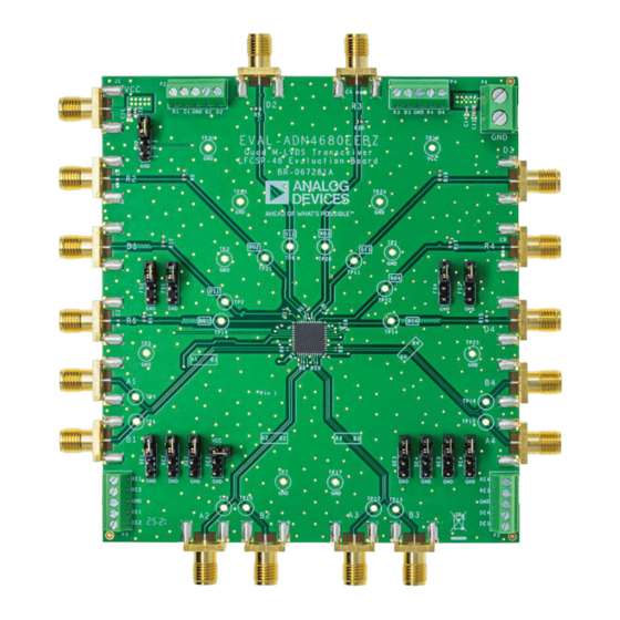
Page 3: Eval-Adn4680Eebz Evaluation Board Photograph
User Guide EVAL-ADN4680E EVAL-ADN4680EEBZ EVALUATION BOARD PHOTOGRAPH Figure 1. analog.com Rev. 0 | 3 of 12... -
Page 4: Evaluation Board Configuration
Connections. to DI4 traces are terminated to GND with 50 Ω resistors, R11, The EVAL-ADN4680EEBZ is powered by connecting a 3.3 V power R13, R16, and R18, respectively. The RO1 to RO4 traces include supply to either the J1 VCC SMA connector or the VCC and GND an optional placeholder for a load capacitor at C2, C8, C4, and connections of the P6 screw terminal block. -
Page 5: Input And Output Connections
User Guide EVAL-ADN4680E EVALUATION BOARD CONFIGURATION Figure 2. Example Evaluation of the ADN4680E Driver and Receiver INPUT AND OUTPUT CONNECTIONS Table 1 details the digital input connections, Table 2 details the digital output connections, and Table 3 details the M-LVDS input and output connections. -
Page 6: Jumper Connections
User Guide EVAL-ADN4680E EVALUATION BOARD CONFIGURATION JUMPER CONNECTIONS Table 4 details the jumper configurations. Table 4. Jumper Configurations Jumper Position Description Connects the ENP pin of the ADN4680E to VCC, which enables global power-up for the device. The state of each transceiver is determined by the DE1 to DE4 and RE1 to RE4 pins. - Page 7 User Guide EVAL-ADN4680E EVALUATION BOARD CONFIGURATION Table 4. Jumper Configurations Jumper Position Description Disconnected Disconnects the DE1 pin from VCC or GND, which allows the DE1 pin to be controlled from the DE1 connection on the P3 screw terminal block. Connects the DE2 pin of the ADN4680E to VCC, which enables the A2 and B2 transmitter if the ENP jumper is connected to VCC.
-
Page 8: Evaluation Board Schematic And Layout
User Guide EVAL-ADN4680E EVALUATION BOARD SCHEMATIC AND LAYOUT Figure 3. EVAL-ADN4680EEBZ Schematic (Page 1) analog.com Rev. 0 | 8 of 12... - Page 9 User Guide EVAL-ADN4680E EVALUATION BOARD SCHEMATIC AND LAYOUT Figure 4. EVAL-ADN4680EEBZ Schematic (Page 2) analog.com Rev. 0 | 9 of 12...
- Page 10 User Guide EVAL-ADN4680E EVALUATION BOARD SCHEMATIC AND LAYOUT Figure 5. EVAL-ADN4680EEBZ Silkscreen Figure 7. EVAL-ADN4680EEBZ Internal Layer 2 (GND) Figure 6. EVAL-ADN4680EEBZ Component Side Figure 8. EVAL-ADN4680EEBZ Internal Layer 3 (VCC) analog.com Rev. 0 | 10 of 12...
- Page 11 User Guide EVAL-ADN4680E EVALUATION BOARD SCHEMATIC AND LAYOUT Figure 9. EVAL-ADN4680EEBZ Solder Side analog.com Rev. 0 | 11 of 12...
-
Page 12: Ordering Information
Evaluation Board until you have read and agreed to the Agreement. Your use of the Evaluation Board shall signify your acceptance of the Agreement. This Agreement is made by and between you (“Customer”) and Analog Devices, Inc. (“ADI”), with its principal place of business at Subject to the terms and conditions of the Agreement, ADI hereby grants to Customer a free, limited, personal, temporary, non-exclusive, non-sublicensable, non-transferable license to use the Evaluation Board FOR EVALUATION PURPOSES ONLY.
Need help?
Do you have a question about the EVAL-ADN4680EEBZ and is the answer not in the manual?
Questions and answers