Table of Contents
Advertisement
Quick Links
One Technology Way
• P.O. Box 9106 • Norwood, MA 02062-9106, U.S.A. • Tel: 781.329.4700 • Fax: 781.461.3113 • www.analog.com
Evaluating the
FEATURES
Isolated ground planes (logic side and bus side)
Convenient connections through SMA terminals
3.3 V or 2.5 V power on Side 1 (V
(V
/V
)
IN2
DD2
Ground on Side 1 (GND
) and Side 2 (GND
1
LVDS input signals: D
, D
IN1+
LVDS output signals: D
OUT1+
Jumper-selectable supply power of 3.3 V or 2.5 V
Termination resistors on all LVDS drivers/receivers
EVALUATION KIT CONTENTS
EVAL-ADN4651EB1Z
or
EVAL-ADN4652EB1Z
DOCUMENTS NEEDED
ADN4650/ADN4651/ADN4652
EQUIPMENT NEEDED
Signal generator
Oscilloscope
PLEASE SEE THE LAST PAGE FOR AN IMPORTANT
WARNING AND LEGAL TERMS AND CONDITIONS.
EVAL-ADN4651EB1Z/EVAL-ADN4652EB1Z
ADN4651/ADN4652
/V
) and Side 2
IN1
DD1
)
2
, D
, D
IN1−
IN2+
IN2−
, D
, D
, D
OUT1−
OUT2+
OUT2−
evaluation board
data sheet
5 kV RMS, 600 Mbps LVDS Isolator (SOIC_W)
GENERAL DESCRIPTION
The
EVAL-ADN4651EB1Z
quick and easy evaluation of the
differential signalling (LVDS) isolator without the need for external
components. The
Inc., iCoupler® technology to combine a 2-channel isolator with an
LVDS receiver and driver into a single, 20-lead wide body SOIC
package. They are capable of running at data rates of up to 600
Mbps with very low jitter.
The evaluation board has separate ground and power planes for
each side of the isolator. This separation enables the evaluation
of the
ADN4651/ADN4652
sides of the device. Jumper-selectable power supplies at 3.3 V or
2.5 V are required on each side of the ADN4651/ADN4652. Using
an on-chip LDO, 2.5 V can be provided from an external 3.3 V
power supply.
Complete information about the
available in the
which should be consulted in conjunction with this user guide
when using the evaluation boards.
Rev. A | Page 1 of 13
User Guide
and
EVAL-ADN4652EB1Z
ADN4651/ADN4652
ADN4651/ADN4652
employ Analog Devices,
with galvanic isolation between both
ADN4651/ADN4652
ADN4650/ADN4651/ADN4652
allow
low-voltage
is
data sheet,
Advertisement
Table of Contents

Subscribe to Our Youtube Channel
Related Manuals for Analog Devices EVAL-ADN4651EB1Z


Summary of Contents for Analog Devices EVAL-ADN4651EB1Z
-
Page 1: Features
3.3 V or 2.5 V power on Side 1 (V ) and Side 2 components. The ADN4651/ADN4652 employ Analog Devices, Ground on Side 1 (GND ) and Side 2 (GND Inc., iCoupler® technology to combine a 2-channel isolator with an... -
Page 2: Table Of Contents
UG-900 EVAL-ADN4651EB1Z/EVAL-ADN4652EB1Z User Guide TABLE OF CONTENTS Features ....................1 Setting Up the Evaluation Board ..........4 Evaluation Kit Contents ..............1 Radiated Emissions Test Results (EN 55022) ........6 Documents Needed ................1 Evaluation Board Schematic and Artwork ........8 ... -
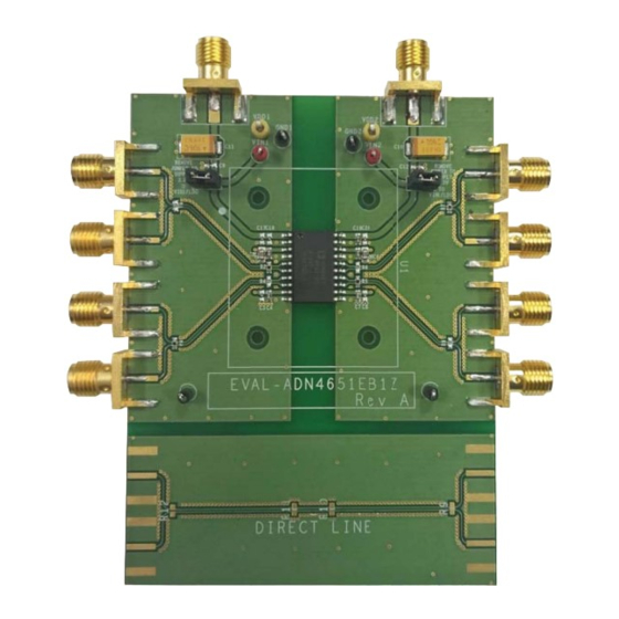
Page 3: Adn4651 And Adn4652 Evaluation Board Photographs
EVAL-ADN4651EB1Z/EVAL-ADN4652EB1Z User Guide UG-900 EVALUATION BOARD PHOTOGRAPHS Figure 1. EVAL-ADN4651EB1Z Evaluation Board Figure 2. EVAL-ADN4652EB1Z Evaluation Board Rev. A | Page 3 of 13... -
Page 4: Evaluation Board Configuration
Figure 5 (signal generator and oscilloscope connections are reversed for EVAL-ADN4652EB1Z, per Table 2 and Table 3). SMA connectors expose all LVDS inputs and outputs for the EVAL-ADN4651EB1Z, but are reversed for the EVAL- ADN4652EB1Z (see Table 2 and Table 3). Connect a signal... - Page 5 SUPPLY OSCILLOSCOPE GND1 GND2 GND1 GND2 EVAL-ADN4651EB1Z Figure 5. Basic LVDS Isolator Evaluation Board Operation for the EVAL-ADN4651EB1Z; Scope and Signal Generator Reversed for the EVAL-ADN4652EB1Z Table 1. Jumper Configuration Jumper Position Description Open 3.3 V power supply connected to Connector J9 for V Closed 2.5 V power supply connected to Connector J9, V...
-
Page 6: Changes To Figure 6 Caption And Radiated Emissions Test Results (En 55022) Section
2. INPUT SIGNAL: |V | = 300mV, V = 1.1V, 600MBPS PRBS7 OR 300MHz CLOCK Figure 6. Test Setup for EN 55022 Radiated Emissions Testing for the EVAL-ADN4651EB1Z; Scope and Signal Generator Reversed for the EVAL-ADN4652EB1Z Radiated emissions testing is performed with the... - Page 7 EVAL-ADN4651EB1Z/EVAL-ADN4652EB1Z User Guide UG-900 1000 FREQUENCY (MHz) Figure 7. EVAL-ADN4651EB1Z Radiated Emissions (Horizontal, Peak, 30 MHz to 1 GHz) with 600 Mbps PRBS7 Input 1000 FREQUENCY (MHz) Figure 8. EVAL-ADN4651EB1Z Radiated Emissions (Vertical, Peak, 30 MHz to 1 GHz) with 600 Mbps PRBS7 Input...
-
Page 8: Added Figure 11 And Figure 12
UG-900 EVAL-ADN4651EB1Z/EVAL-ADN4652EB1Z User Guide EVALUATION BOARD SCHEMATIC AND ARTWORK AGND3 VIN2 VIN1 VDD1 VDD2 TP40 DECOUPLING AGND2 AGND1 AGND1 VIN1 VIN2 VDD1 AGND2 AGND1 AGND2 AGND1 AGND2 20PIN SOICWB TP41 TP42 5001 1 5001 1 AGND1 AGND1 AGND2 AGND2 AGND1 AGND2 Figure 9. - Page 9 EVAL-ADN4651EB1Z/EVAL-ADN4652EB1Z User Guide UG-900 AGND3 VIN2 VIN1 VDD1 VDD2 TP40 DECOUPLING AGND2 AGND1 AGND1 VIN1 VIN2 VDD1 AGND2 AGND1 AGND2 AGND1 AGND2 20PIN SOICWB TP41 TP42 5001 1 5001 1 AGND1 AGND2 AGND2 AGND1 AGND1 AGND2 Figure 11. EVAL-ADN4652EB1Z Schematic Figure 12.
- Page 10 UG-900 EVAL-ADN4651EB1Z/EVAL-ADN4652EB1Z User Guide Figure 13. EVAL-ADN4651EB1Z/EVAL-ADN4652EB1Z Component Side Figure 14. EVAL-ADN4651EB1Z/EVAL-ADN4652EB1Z Inner Layer 2, Ground Rev. A | Page 10 of 13...
- Page 11 EVAL-ADN4651EB1Z/EVAL-ADN4652EB1Z User Guide UG-900 Figure 15. EVAL-ADN4651EB1Z/EVAL-ADN4652EB1Z Inner Layer 3, Power Figure 16. EVAL-ADN4651EB1Z/EVAL-ADN4652EB1Z Solder Side Rev. A | Page 11 of 13...
-
Page 12: Added Table 6; Renumbered Sequentially
UG-900 EVAL-ADN4651EB1Z/EVAL-ADN4652EB1Z User Guide ORDERING INFORMATION BILL OF MATERIALS Table 5. Bill of Materials for the EVAL-ADN4651EB1Z Qty. Reference Designator Description Manufacturer Part Number C1, C4, C5, C7 Capacitors, 100 nF, 0402 Multicomp MC0402X104K100CT C2, C6 Capacitors, 1 µF, 0603... - Page 13 By using the evaluation board discussed herein (together with any tools, components documentation or support materials, the “Evaluation Board”), you are agreeing to be bound by the terms and conditions set forth below (“Agreement”) unless you have purchased the Evaluation Board, in which case the Analog Devices Standard Terms and Conditions of Sale shall govern. Do not use the Evaluation Board until you have read and agreed to the Agreement.
Need help?
Do you have a question about the EVAL-ADN4651EB1Z and is the answer not in the manual?
Questions and answers