Table of Contents
Advertisement
Quick Links
FEATURES
10 column × 8 rows port expander, maximum 10 × 8 keypad
matrix
Rows and columns configurable to keypad, GPI or GPO
Dual light sensor inputs
2
I
C interface
Auto increment capability
1.8 V and 3.0 V operation for I
Interrupt capability
ADP5588 evaluation software included
On-board reset
GPO indicator LEDs
GPIO jumper configuration
Switches to set GPI levels
GENERAL DESCRIPTION
The ADP5588 demonstration board is used to exercise the
features of the ADP5588 keypad/GPIO expander IC. It consists
of a daughterboard and a motherboard. The motherboard houses
the keypad (80 switches), a USB connector (JP1), a reset switch
(S17), and all the hardware necessary to power the IC and establish
USB communication with the PC. Two 20-pin connectors (J11
and J12) are used to plug in the daughterboard. The ADP5588
IC is mounted on the daughterboard along with the LK1 and LK2
jumpers, which are used to insert or remove the C19 and C20
capacitors from the light sensor comparator circuitry.
Rev. 0
Evaluation boards are only intended for device evaluation and not for production purposes.
Evaluation boards are supplied "as is" and without warranties of any kind, express, implied, or
statutory including, but not limited to, any implied warranty of merchantability or fitness for a
particular purpose. No license is granted by implication or otherwise under any patents or other
intellectual property by application or use of evaluation boards. Information furnished by Analog
Devices is believed to be accurate and reliable. However, no responsibility is assumed by Analog
Devices for its use, nor for any infringements of patents or other rights of third parties that may result
from its use. Analog Devices reserves the right to change devices or specifications at any time
without notice. Trademarks and registered trademarks are the property of their respective owners.
Evaluation boards are not authorized to be used in life support devices or systems.
2
C and GPIOs (1.7 V ~ 3.0 V)
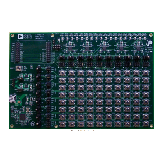
MOTHERBOARD LAYOUT
DAUGHTER
ALS JUMPER
BOARD
CONNECTORS
RESET SWITCH
USB CONNCTOR
ADP5588 Keypad I/O Expander
The demonstration board assembly is powered either via J10 or
the USB port and comes with a free graphical user interface (GUI)
to exercise the ADP5588 features. In addition to the keypad
switches, the motherboard also has 18 GPO LED indicators (D1
through D11, D22 through D27, and D30), power status LEDs
(D19 and D21), a 2.7 V regulator, a 3.3 V regulator, and jumpers
(J1 through J8 and J13 through J22) to configure the GPIOs as
GPIs, GPOs, or keypad lines. The motherboard is equipped with
jumpers (LK8 and LK10) to configure the board to use either
external regulated voltages via J10 or the on-board regulators when
plugged into the USB port. When using the USB port as the power
source, place jumpers across Pin 1 and Pin 2 of LK8 and LK10.
When using external voltages, place jumpers across Pin 2 and
Pin 3 of LK8 and LK10. V
and V
(Pin 1 of J10) should be 3.3 V.
BOARD
A set of switches (SW1 through SW18) provides logic high
(Logic 1) or logic low (Logic 0) drives to the GPIOs configured
as GPIs. Column 8 and Column 9 of the IC have an additional
jumper (J9) that allows the user to configure theses lines into
light sensor comparator inputs. Place a jumper across Pin 1 and
Pin 3 of J9 and another across Pin 2 and Pin 4 of J9 to configure
these pins as Keypad Column 8 and Keypad Column 9, or place
a jumper across Pin 3 and Pin 5 of J9 and another across Pin 4
and Pin 6 of J9 to configure these pins as light sensor inputs.
GPO LEDs
GPI SWITCHES
GPIO JUMPER SETTINGS
KEYPAD SWITCHES
Figure 1.
One Technology Way, P.O. Box 9106, Norwood, MA 02062-9106, U.S.A.
Tel: 781.329.4700
Fax: 781.461.3113
Evaluation Board
EVAL-ADP5588
(Pin 3 of J10) should be 1.8 V to 3.0 V,
CC
www.analog.com
©2009 Analog Devices, Inc. All rights reserved.
Advertisement
Chapters
Table of Contents

Related Manuals for Analog Devices ADP5588


Summary of Contents for Analog Devices ADP5588
-
Page 1: Features
Devices for its use, nor for any infringements of patents or other rights of third parties that may result One Technology Way, P.O. Box 9106, Norwood, MA 02062-9106, U.S.A. from its use. Analog Devices reserves the right to change devices or specifications at any time Tel: 781.329.4700 www.analog.com... -
Page 2: Table Of Contents
Ordering Information ..............19 Software Installation ................. 4 Bill of Materials (BOM) ............. 19 ADP5588 Evaluation Installation ..........4 Ordering Guide ................20 LabVIEW Runtime Engine Installation ........5 ESD Caution................20 REVISION HISTORY 6/09—Revision 0: Initial Version... -
Page 3: Demonstration Board Assembly
EVAL-ADP5588 DEMONSTRATION BOARD ASSEMBLY Figure 2. Daughterboard Figure 3. Motherboard Rev. 0 | Page 3 of 20... -
Page 4: Software Installation
EVAL-ADP5588 SOFTWARE INSTALLATION Installation of the LabVIEW_Runtime_Engine.exe file and the ADP5588 GUI is required before using the ADP5588 demonstration board. ADP5588 EVALUATION INSTALLATION To run these installations, do the following: Insert the ADP5588 evaluation CD and run the ADP5588 Setup.exe file. When the screen in Figure 4 appears, click Next >. -
Page 5: Labview Runtime Engine Installation
EVAL-ADP5588 When the screen in Figure 12 appears, click Next>> to start the NI LabVIEW 8.2 Runtime Engine installation. Figure 9. InstallShield Wizard Complete LABVIEW RUNTIME ENGINE INSTALLATION The LabVIEW Runtime Engine comes as a self-extracting Figure 12. NI LabVIEW 8.2 Runtime Engine Installation archive and must be unzipped before installation. -
Page 6: Usb Driver Installation
USB port after software installation. When assembly is complete, do the following to install the USB drivers. Plug the ADP5588 board into the computer using the provided USB cable. When the system recognizes the board, the screen shown in Figure 19 appears. -
Page 7: Using The Software
USING THE SOFTWARE Anyway; this completes the USB driver installation. Before running the software, make sure that the ADP5588 board assembly is plugged into the USB port. When it is plugged in properly, the two supply LEDs (D19 and D21) light up. - Page 8 Keypad Configuration To program a GPIO pin as a keypad in the GPIO tab: The ADP5588 has eighteen GPIOs that can be programmed as Set the bits for the columns and rows that need to be keypad lines to make up a 10 × 8 keypad matrix (80 keys). If a...
- Page 9 Define the trigger level for any of the rows or columns for which interrupt is enabled (Register 0x26 through The ADP5588 allows the user to configure any of the eighteen Register 0x28). GPIOs as GPIs or GPOs (see Figure 24).
- Page 10 EVAL-ADP5588 GPO Configuration Columns or rows configured as GPO are not read into Register 0x014, Register 0x15, and Register 0x16. The D1 To GPO configure a row or column, do the following: through D11, D22 through D27, and D30 status LED indicate Clear the bit for the row or column that needs to be the level of the GPIOs configured as GPOs.
- Page 11 Set Bit 2 and/or Bit 3 of Register 0x30 to enable interrupt for the comparators, if needed. The ADP5588 is equipped to support two light sensor comparator Set Bit 0 and Bit 1 of Register 0x31 and Register 0x32 to inputs.
- Page 12 EVAL-ADP5588 Figure 26. History Tab History The script file allows the user to program all the register settings without having to repeat these commands one by one. This The History tab is used to record command sequences that can feature can be used to automate certain functions that will be be used later as script files.
-
Page 13: Schematics
EVAL-ADP5588 SCHEMATICS LK3 1 Way Link LK3 1 Way Link 1UF/16V 1UF/16V LK1 1 Way Link LK1 1 Way Link 0.1UF 0.1UF INTb Row7 Row7 Col9_Sens2 Row6 Row5 Row2 Col8_Sens1 Row6 Row4 Row1 Row3 Row0 Row5 Col7 Row4 Col6 LK2 1 Way Link... - Page 14 EVAL-ADP5588 Figure 28. Daughterboard Layout (Top Layer) Figure 29. Daughterboard Layout (Bottom Layer) Rev. 0 | Page 14 of 20...
- Page 15 EVAL-ADP5588 Figure 30. Motherboard Schematic Rev. 0 | Page 15 of 20...
-
Page 16: Vcc Vcc
EVAL-ADP5588 EXT_VBOARD 2 Way Link 2 Way Link VBOARD 10uF 10uF CON4 CON4 0.1uF 0.1uF 100k 100k 0.1uF 0.1uF VBOARD VBOARD EXT_VCC LK10 LK10 2 Way Link 2 Way Link 0.1uF 0.1uF 6.2pF 6.2pF 100k 100k VBOARD RDY0/SLRD RESET RDY1/SLWR... -
Page 17: Row4
EVAL-ADP5588 Figure 32. Motherboard Layout (Top Layer) Table 1. Keypad Translation Table Col 0 Col 1 Col 2 Col 3 Col 4 Col 5 Col 6 Col 7 Col 8 Col 9 Row0 1/A0 2/B0 3/C0 4/D0 5/E0 6/F0 7/G0... - Page 18 EVAL-ADP5588 Figure 33. Motherboard Layout (Bottom Layer) Rev. 0 | Page 18 of 20...
-
Page 19: Ordering Information
EVAL-ADP5588 ORDERING INFORMATION BILL OF MATERIALS (BOM) Table 2. Daughterboard BOM Item Quantity Reference Designator Description Manufacturer/Vendor Manufacturer Part No. ADP5588 IC Analog Devices ADP5588ACPZ-RL C19, C20 0.1 μF capacitor Murata GRM188R71E104KA01 1 μF capacitor Murata GRM188R61C105K J1, J2 10 × 2 connector... -
Page 20: Ordering Guide
ORDERING GUIDE ESD CAUTION Model Temperature Range ADP5588-EVALZ Evaluation Board Z = RoHS Compliant Part. ©2009 Analog Devices, Inc. All rights reserved. Trademarks and registered trademarks are the property of their respective owners. EB08102-0-6/09(0) Rev. 0 | Page 20 of 20...
Need help?
Do you have a question about the ADP5588 and is the answer not in the manual?
Questions and answers