Table of Contents
Advertisement
Quick Links
One Technology Way • P.O. Box 9106 • Norwood, MA 02062-9106, U.S.A. • Tel: 781.329.4700 • Fax: 781.461.3113 • www.analog.com
Evaluation Board for the
FEATURES
Plug and play energy harvesting platform
Compatible with Analog Devices, Inc., wireless sensor
network (WSN) platform
Solar panel harvester included
One regulated output with programmable output voltage
RoHS compliant
GENERAL DESCRIPTION
The
ADP5091
demonstration platform is a plug and play
evaluation board (ADP5091-2-EVALZ) for energy harvesting.
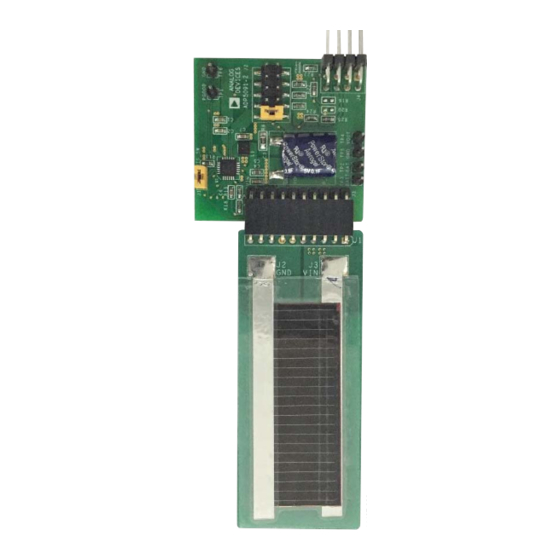
The evaluation board includes the photovoltaic (PV) panel and
all of the power management to enable devices to be powered
using energy harvesting. It is based on the Alta Device PV cell
and the
ADP5091
energy harvesting power management IC.
The demonstration platform converts light energy to electrical
energy. The PV panel converts the light to 0.8 V electrical
energy. The
ADP5091
boosts the input voltage from 0.8 V to
3.5 V and stores the energy in a supercapacitor.
PLEASE SEE THE LAST PAGE FOR AN IMPORTANT
WARNING AND LEGAL TERMS AND CONDITIONS.
ADP5091
Demonstration Platform for Energy Harvesting
SYSTEM BLOCK DIAGRAM
ENERGY HARVESTING
POWER MANAGEMENT
SOLAR PV PANEL
ADP5091
ENERGY STORAGE
SUPERCAP
Rev. 0 | Page 1 of 9
ADP5091-2-EVALZ User Guide
The
ADP5091
has a regulated output with programmable output
voltage. By combining a low dropout (LDO) regulator and a boost
regulator, it offers a more compatible output voltage than the
output of a main boost regulator. The Alta Device PV cell is a
light harvesting, dye sensitized PV cell. It is optimized for indoor
environments, where lux levels of 200 lux to 1000 lux are typical.
The
ADP5091
is an ultralow power, synchronous, boost dc-to-dc
regulator. The
ADP5091
3.3 V and provides a high efficiency solution with integrated
power switch, synchronous rectifier, battery management, and
one regulated output. The demonstration platform provides an
easy way to evaluate the device.
Full details about the
sheet, which should be consulted in conjunction with this user
guide when using the ADP5091-2-EVALZ.
The system also plugs directly into the Analog Devices WSN
demonstration platform.
This user guide describes how to set up the board and how to
use it for powering loads.
OUTPUT CONNECTOR
BACKUP BATTERY
Figure 1.
runs from input voltages of 0.38 V to
ADP5091
are available in the product data
UG-927
Advertisement
Table of Contents

Subscribe to Our Youtube Channel
Related Manuals for Analog Devices ADP5091-2-EVALZ


Summary of Contents for Analog Devices ADP5091-2-EVALZ
-
Page 1: Features
IC. guide when using the ADP5091-2-EVALZ. The demonstration platform converts light energy to electrical The system also plugs directly into the Analog Devices WSN energy. The PV panel converts the light to 0.8 V electrical demonstration platform. -
Page 2: Table Of Contents
UG-927 ADP5091-2-EVALZ User Guide TABLE OF CONTENTS Features ....................1 Power Management of the Output (LDO) .........4 General Description ................. 1 J4 Output Connector ..............5 System Block Diagram ..............1 Evaluation Board Schematics ............6 ... -
Page 3: Evaluation Board Quick Start Guide
ADP5091-2-EVALZ User Guide UG-927 EVALUATION BOARD QUICK START GUIDE This section explains how to connect the solar panel to the Connect J2_1 and J2_2 on the evaluation board, as shown evaluation board and how to configure the evaluation board to in Figure 3. -
Page 4: Evaluation Board Hardware
LDO can generate different output voltages. Table 1 shows the Figure 7. Jumper Position on Evaluation Board for Setting 4 jumper connections and the corresponding output voltage on the ADP5091-2-EVALZ. See the Evaluation Board Schematic section for more details. Figure 8. Jumper Position on Evaluation Board for Setting 5 Figure 4. -
Page 5: J4 Output Connector
The evaluation board is directly compatible with PGOOD pin (Pin 2) high. It is connected to the host MCU the Analog Devices WSN demonstration boards. Table 2 shows general-purpose input/output (GPIO) input. See the the pinout of the J4 output connector and a brief description of... -
Page 6: Evaluation Board Schematics
UG-927 ADP5091-2-EVALZ User Guide EVALUATION BOARD SCHEMATICS Figure 13. ADP5091-2-EVALZ Evaluation Board Schematic Figure 14. ADP5091-2-EVALZ PV Board Schematic Rev. 0 | Page 6 of 9... -
Page 7: Evaluation Board Layout
ADP5091-2-EVALZ User Guide UG-927 EVALUATION BOARD LAYOUT Figure 15. Top Assembly Figure 16. Bottom Assembly Rev. 0 | Page 7 of 9... -
Page 8: Ordering Information
UG-927 ADP5091-2-EVALZ User Guide ORDERING INFORMATION BILL OF MATERIALS Table 3. Bill of Materials of Evaluation Board Reference Designator Description Part Number Vendor CR2032 holder BC2032-F1 Memory Protection Devices C1, C4 0.1 μF capacitors, C0603 GRM188R71H104KA93 Murata C2, C5 4.7 μF, 10 V capacitors, C0603... - Page 9 By using the evaluation board discussed herein (together with any tools, components documentation or support materials, the “Evaluation Board”), you are agreeing to be bound by the terms and conditions set forth below (“Agreement”) unless you have purchased the Evaluation Board, in which case the Analog Devices Standard Terms and Conditions of Sale shall govern. Do not use the Evaluation Board until you have read and agreed to the Agreement.
Need help?
Do you have a question about the ADP5091-2-EVALZ and is the answer not in the manual?
Questions and answers