Advertisement
Quick Links
One Technology Way • P.O. Box 9106 • Norwood, MA 02062-9106, U.S.A. • Tel: 781.329.4700 • Fax: 781.461.3113 • www.analog.com
FEATURES
Wide input voltage range: 2.75 V to 18 V
Bias input voltage range: 4.5 V to 18 V
Full-featured evaluation board for the
Channel 1 and Channel 2: 7 A synchronous buck regulator,
or 14 A output in parallel operation
Channel 3: 3 A synchronous buck regulator
Selective PSM or FPWM operation
Programmable switching frequency from 2.5 MHz to 250 kHz
Frequency synchronization input or output
PLEASE SEE THE LAST PAGE FOR AN IMPORTANT
WARNING AND LEGAL TERMS AND CONDITIONS.
Evaluating the
Triple Buck Regulator Integrated Power Solution
ADP5056
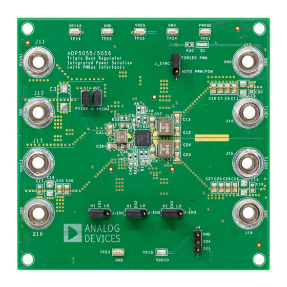
ADP5056-EVALZ PHOTOGRAPH
ADP5056-EVALZ
ADP5056
GENERAL DESCRIPTION
This user guide describes the evaluation of the
includes detailed schematics and printed circuit board (PCB)
layouts.
The ADP5056-EVALZ features the ADP5056, which combines
three high performance buck regulators in a 43-terminal land
grid array (LGA) to meet the demanding performance and
board space requirements. The ADP5056-EVALZ connects to
input voltages up to 18 V directly, without any preregulators.
Full details on the device are provided in the
sheet, available from Analog Devices, Inc. Consult this data
sheet in conjunction with this user guide when evaluating the
ADP5056.
Figure 1.
Rev. 0 | Page 1 of 11
User Guide
UG-1517
ADP5056
and
ADP5056
data
Advertisement

Related Manuals for Analog Devices ADP5056-EVALZ


Summary of Contents for Analog Devices ADP5056-EVALZ
- Page 1 Frequency synchronization input or output Full details on the device are provided in the ADP5056 data sheet, available from Analog Devices, Inc. Consult this data sheet in conjunction with this user guide when evaluating the ADP5056. ADP5056-EVALZ PHOTOGRAPH Figure 1.
- Page 2 Features ....................1 Quick Startup .................4 General Description ................. 1 Measuring Evaluation Board Performance ........5 ADP5056-EVALZ Photograph ............1 Measuring Output Voltage Ripple of the Buck Regulator ..5 Revision History ................2 Measuring the Switching Waveform of the Buck Regulator..5 Evaluation Board Hardware ............
- Page 3 18 V. If separate power supplies are used for PVIN1 and VBIAS output load: with R35 removed (on the ADP5056-EVALZ, PVIN1 and VBIAS are connected together through the R35, 0 Ω resistor by default), Ensure that the evaluation board is turned off before the input voltage range for the three buck regulators is 2.75 V to...
- Page 4 UG-1517 ADP5056-EVALZ User Guide Connect the voltmeter positive terminal measuring the When the power source and load are connected to the evaluation output voltage of the Channel 1 buck regulator to J14 board, the evaluation board can be powered for operation. If the (VOUT1), and connect the voltmeter negative terminal load is not enabled, enable the load.
- Page 5 ADP5056-EVALZ User Guide UG-1517 MEASURING EVALUATION BOARD PERFORMANCE MEASURING OUTPUT VOLTAGE RIPPLE OF THE EVALUATING EFFICIENCY BUCK REGULATOR Measure the efficiency, η, by comparing the input power with To observe the output voltage ripple of Channel 1, place an the output power.
- Page 6 PVIN1 Operation Channel 1 and Channel 2 are configured as individual outputs CHANNEL 1 OUT1 on the ADP5056-EVALZ by default. To configure Channel 1 BUCK REGULATOR and Channel 2 to operate in interleaved parallel single output mode, follow these steps: •...
- Page 7 ADP5056-EVALZ User Guide UG-1517 EVALUATION BOARD SCHEMATICS AND ARTWORK Figure 5. Evaluation Board Schematic of the ADP5056 Rev. 0 | Page 7 of 11...
- Page 8 UG-1517 ADP5056-EVALZ User Guide Figure 6. Top Layer, Recommended Layout for ADP5056 Figure 7. Second Layer, Recommended Layout for ADP5056 Rev. 0 | Page 8 of 11...
- Page 9 ADP5056-EVALZ User Guide UG-1517 Figure 8. Third Layer, Recommended Layout for ADP5056 Figure 9. Bottom Layer, Recommended Layout for ADP5056 Rev. 0 | Page 9 of 11...
- Page 10 UG-1517 ADP5056-EVALZ User Guide ORDERING INFORMATION BILL OF MATERIALS Table 4. Qty. Reference Designator Description Manufacturer Part Number Murata GRM188C81E475KE11 Ceramic capacitor, 4.7 µF, X6S, 25 V, 10%, 0603 Ceramic capacitor, 4.7 µF, X6S, 6.3 V, 20%, Murata GRM155C80J475MEAA 0402...
- Page 11 By using the evaluation board discussed herein (together with any tools, components documentation or support materials, the “Evaluation Board”), you are agreeing to be bound by the terms and conditions set forth below (“Agreement”) unless you have purchased the Evaluation Board, in which case the Analog Devices Standard Terms and Conditions of Sale shall govern. Do not use the Evaluation Board until you have read and agreed to the Agreement.
Need help?
Do you have a question about the ADP5056-EVALZ and is the answer not in the manual?
Questions and answers