ST STM8S Getting Started
Hide thumbs
Also See for STM8S:
- Reference manual (449 pages) ,
- Application note (42 pages) ,
- User manual (23 pages)
Table of Contents
Advertisement
Quick Links
AN2752
Application note
Getting started with STM8S and STM8AF microcontrollers
Introduction
This application note complements the information contained in STM8S and STM8AF
datasheets by describing the minimum hardware and software environment required to build
an application around these 8-bit microcontrollers.
This document also contains detailed reference design schematics with descriptions of the
main components, and some hardware recommendations.
Some of the information given in
Section 9: Software toolchain
and
Section 10: Setting up
the development environment
has a wider scope, to know if it applies to STM8 MCUs
different from those of the STM8S and STM8AF Series contact your local representative.
April 2018
AN2752 Rev 6
1/40
www.st.com
1
Advertisement
Table of Contents

Related Manuals for ST STM8S


Summary of Contents for ST STM8S
- Page 1 Section 9: Software toolchain Section 10: Setting up the development environment has a wider scope, to know if it applies to STM8 MCUs different from those of the STM8S and STM8AF Series contact your local representative. April 2018 AN2752 Rev 6 1/40...
-
Page 2: Table Of Contents
Contents AN2752 Contents Hardware requirements summary ......6 Power supply ..........7 Power supply overview . - Page 3 AN2752 Contents Single wire interface module (SWIM) ......20 8.1.1 SWIM overview ......... . . 20 8.1.2 SWIM connector pins .
- Page 4 List of tables AN2752 List of tables Table 1. Component list ............18 Table 2.
- Page 5 AN2752 List of figures List of figures Figure 1. Power supply ............7 Figure 2.
-
Page 6: Hardware Requirements Summary
Hardware requirements summary AN2752 Hardware requirements summary To build an application based on a microcontroller of the STM8S or STM8AF Series, the board must have at least the following features: • power supply • clock management • reset management •... -
Page 7: Power Supply
AN2752 Power supply Power supply Power supply overview The device can be supplied through a 3.0 V to 5.5 V external source. An on-chip power management system provides the 1.8 V digital supply to the core logic, both in normal and low power modes. -
Page 8: Main Operating Voltages
AN2752 Main operating voltages STM8S and STM8AF devices are made in 0.13 µm technology. The STM8S and STM8AF core and I/O peripherals need different power supplies. In fact, STM8S and STM8AF devices have an internal regulator with a nominal target output of 1.8 V. -
Page 9: Figure 3. Typical Layout Of V
(PCBs). In addition, each power supply pair has to be decoupled with 100 nF filtering ceramic capacitors (C) with one chemical capacitor (1 to 2 µF) in parallel on the STM8S or STM8AF device. The ceramic capacitors (including C... -
Page 10: Analog-To-Digital Converter (Adc)
REF- Analog input STM8S and STM8AF devices have 16 analog input channels, which are converted by the ADC one at a time, and each of them is multiplexed with an I/O. The analog input interface of the ADC is shown in Figure Figure 4. - Page 11 = 0.5 µs (for 2 MHz input CLK) Equation 2 is specific for R and C when designing an analog input interface for the ADC. Refer to the STM8S or STM8AF datasheets and/or to reference manual RM0016 (available on www.st.com) for more details. AN2752 Rev 6 11/40...
-
Page 12: Clock Management
Clock management AN2752 Clock management Clock management overview STM8S and STM8AF devices offer a flexible way of selecting the core and peripheral clocks (ADC, memory, digital peripherals). As shown in Figure 5, these devices have internal and external clock source inputs and one output clock (CCO). -
Page 13: Figure 6. Clock Sources
AN2752 Clock management Figure 6. Clock sources Hardware configuration STM8 (I/O available) External source Frequency: 32 kHz … 24 MHz Comparator hysteresis: 0.1 * V Caution: Without prescaler, a duty cycle of maximum 45/55% must be respected STM8 Load capacitors Frequency range: 1-24 MHz Wake-up time: <... -
Page 14: Reset Control
Reset control AN2752 Reset control Reset management overview The reset cell is a dedicated 5 V bidirectional I/O. Its output buffer driving capability is fixed to Io = 2 mA at 0.4 V in the 3 V to 5.5 V range, which includes a 40 kΩ pull-up. Output buffer is reduced to the n-channel MOSFET (NMOS). -
Page 15: Figure 8. Output Characteristics
AN2752 Reset control Output characteristics • A valid pulse on the pin is guaranteed with a pulse whose duration is higher than 20 ns on the internal output buffer. • After a valid pulse is recognized, a pulse of at least 20 µs is guaranteed on the pin, starting from the falling edge of A. -
Page 16: Recommendations
Recommendations AN2752 Recommendations Printed circuit board For technical reasons, the best option is to use a multi-layer PCB with a separate layer dedicated to V and another layer to V supply, which results in a good decoupling, as well as a good shielding effect. For many applications, economical requirements forbid the use of this type of board. -
Page 17: Other Signals
User options STM8S and STM8AF devices have user option features that can be used for remapping or enabling/disabling an automatic reset or low speed watchdog. For more details refer to the product datasheet. -
Page 18: Reference Design
Reference design Components reference Table 1. Component list Component Reference Quantity Comments Refer to the ‘Pinouts and pin description’ and STM8S or Microcontroller ‘Package characteristics’ sections of the STM8AF datasheets to choose the right package Push button Resistor 10 kΩ... -
Page 19: Schematics
Figure 10. Reference design 1. If pins 22 or 25 are required as GPIO, R1 and R2 has to be removed. 2. V must be within the allowed supply voltage range of the STM8S or STM8AF microcontroller. AN2752 Rev 6 19/40... -
Page 20: Development Tools
Development tools AN2752 Development tools Development tools for STM8S and STM8AF microcontrollers include the STice emulation system supported by a complete software tool package including C compiler, assembler and integrated development environment with high-level language debugger. Single wire interface module (SWIM) 8.1.1... -
Page 21: Hardware Connection
Application board SWIM connector STM8 SWIM cable Caution: It is recommended to place the SWIM header as close as possible to the STM8S or STM8AF device, as this minimizes any possible signal degradation caused by long PCB tracks. Emulator STice 8.2.1... -
Page 22: Stice In Emulation Configuration
• 60-pin or 120-pin cable for connection to the application board Connection adapter • Links the connection flex to the footprint of the STM8S or STM8AF microcontroller Adapter socket • Package-specific socket for connection adapter and STM8S or STM8AF microcontroller 8.2.2... -
Page 23: In-Circuit Programming And Debugging
I/O. In both the emulation and the in-circuit programming/debugging configuration, STice is driven by the ST visual develop (STVD) or ST visual programmer (STVP) integrated development environment running on the host PC. This provides total control of advanced application building, debugging and programming features from a single easy-to-use interface. -
Page 24: Figure 15. In-Circuit Programming And Debugging
Figure 15. In-circuit programming and debugging ICD/ICP flat cable connects STice to microcontroller via ICD/ICP connector on application board SWIM connector linked to microcontroller (SWIM protocol for STM8, or ICC protocol for ST) ST microcontroller on application board 24/40 AN2752 Rev 6... -
Page 25: Software Toolchain
AN2752 Software toolchain Software toolchain To write, compile and run the first software on an STM8S or STM8AF device, the following components of the software toolchain are required (see Figure 16): • Integrated development environment • Compiler • Firmware library (optional, used to ease the start-up) Figure 16. -
Page 26: Integrated Development Environment
STVD is delivered as part of the free ST toolset, which also includes the ST visual programmer (STVP) programming interface and the ST assembler linker. -
Page 27: Firmware Library
AN2752 Software toolchain Firmware library The firmware library is a complete set of source code examples for each peripheral. It is written in strict ANSI-C and it is fully MISRA C 2004 compliant (see Figure 17). All examples are delivered with workspace and project definition files for STVD and Cosmic C compiler, which enables the user to load and compile them easily into the development environment. -
Page 28: Setting Up The Development Environment
Setting up the development environment AN2752 Setting up the development environment The development environment for STM8S and STM8AF microcontroller setup looks different, depending upon the supplier of the software (SW) and upon the hardware (HW) tools. Typical setups are described below for the following SW and HW tools: •... -
Page 29: Using The Tools
Setting up the development environment 10.2 Using the tools Once the tools installation is complete, the ST visual develop (STVD) integrated development environment can be launched. The user then has the choice to generate either a new workspace with a new project or to open an existing workspace. -
Page 30: Project Editing
Setting up the development environment AN2752 10.2.1 Project editing All project source files are visible and can be edited (see Figure 19). Figure 19. STVD MCU edit mode 30/40 AN2752 Rev 6... -
Page 31: Online Help
AN2752 Setting up the development environment 10.2.2 Online help An online help manual is available inside the firmware installation directory (see Figure to help the user understand the structure of the STM8 firmware library. Figure 20. STM8 firmware library on-line help manual AN2752 Rev 6 31/40... -
Page 32: Running The Demonstration Software
Setting up the development environment AN2752 10.3 Running the demonstration software To run the demonstration software on the STM8 evaluation board, the project has to be compiled and the correct HW tool must be selected before the debug session can be started. -
Page 33: Selecting The Correct Debug Instrument
AN2752 Setting up the development environment 10.3.2 Selecting the correct debug instrument In the example below, the Rlink tool is used for communicating via the SWIM interface with the on-board debug module of the STM8. The Rlink tool can be selected from the Debug Instrument Selection list in the Debug Instrument Settings dialog (see Figure 22). -
Page 34: Connecting The Hardware
Setting up the development environment AN2752 10.3.3 Connecting the hardware The Rlink tool can be connected to the PC by a standard USB connection. It is also powered by the USB interface. On the controller side the connection to the STM8 evaluation board is made by the SWIM interface cable. -
Page 35: Starting The Debug Session
AN2752 Setting up the development environment 10.3.4 Starting the debug session Debug mode can be entered by the command ‘Debug Start Debugging’ (see Figure 24). Figure 24. STVD: Starting the debug session AN2752 Rev 6 35/40... -
Page 36: Running The Software
Setting up the development environment AN2752 10.3.5 Running the software After entering debug mode, the software can be started by the run command in the menu ‘Debug Run’ (see Figure 25). Figure 25. STVD: Running the software 36/40 AN2752 Rev 6... -
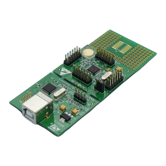
Page 37: Follow Up
Figure 26. STM8 evaluation board 10.3.6 Follow up Step by step, additional peripherals of STM8S and STM8AFdevices can be run, following on from the initial debug session described above. Many features of STM8S and STM8AFdevices are supported by dedicated hardware on the STM8 evaluation board. -
Page 38: Documentation And On-Line Support
STM8AFdatasheets: – STM8AF52xx STM8AF6269/8x/Ax STM8AF51xx STM8AF6169/7x/8x/9x/Ax – STM8AF622x/4x STM8AF6266/68 STM8AF612x/4x STM8AF6166/68 • How to program STM8S and STM8AF Flash program memory and data EEPROM (PM0051) • STM8S and STM8AF microcontroller families reference manual (RM0016) • STM8 CPU programming manual (PM0044) Tools •... -
Page 39: Revision History
Figure 10: Reference design on page 19: updated the value of the C4 capacitor. Added STM8A throughout the document as this revision covers STM8A devices. Replaced “Root part number 2” with STM8S and STM8A. Updated Section 2.2: Main operating voltages: removed Table 1:... - Page 40 ST products and/or to this document at any time without notice. Purchasers should obtain the latest relevant information on ST products before placing orders. ST products are sold pursuant to ST’s terms and conditions of sale in place at the time of order acknowledgement.
Need help?
Do you have a question about the STM8S and is the answer not in the manual?
Questions and answers