Table of Contents
Advertisement
Quick Links
www.ti.com
User's Guide
LMK5B33216EVM User's Guide
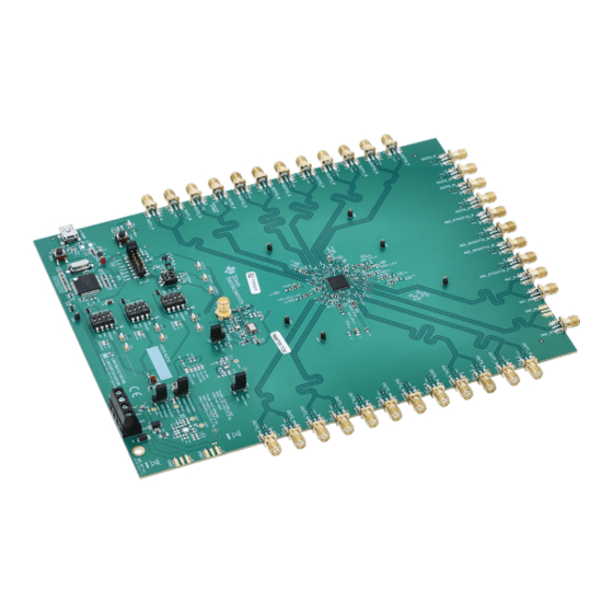
The LMK5B33216EVM is an evaluation module for the LMK5B33216 Network Clock Generator and
Synchronizer. The EVM can be used for device evaluation, compliance testing, and system prototyping.
1
Introduction.............................................................................................................................................................................2
Start......................................................................................................................................................................4
Configuration..................................................................................................................................................................6
3.1 Power Supply.....................................................................................................................................................................
3.2 Logic Inputs and Outputs...................................................................................................................................................
3.3 Switching Between I2C and SPI......................................................................................................................................
3.4 Generating SYSREF Request..........................................................................................................................................
3.5 XO Input...........................................................................................................................................................................
Inputs....................................................................................................................................................13
Outputs...................................................................................................................................................................13
3.8 Status Outputs and LEDS................................................................................................................................................
3.9 Requirements for Making Measurements........................................................................................................................
4 EVM Schematics...................................................................................................................................................................
4.1 Power Supply Schematic.................................................................................................................................................
4.2 Alternative Power Supply Schematic...............................................................................................................................
4.3 Power Distribution Schematic..........................................................................................................................................
4.4 LMK5B33216 and Input Reference Inputs IN0 to IN1 Schematic....................................................................................
4.8 XO Schematic..................................................................................................................................................................
4.9 Logic I/O Interfaces Schematic........................................................................................................................................
Schematic.....................................................................................................................................................23
Materials.............................................................................................................................................................24
5.1 Loop Filter and Vibration Nonsensitive Capacitors..........................................................................................................
6.1 Using the Start Page........................................................................................................................................................
6.2 Using the Status Page.....................................................................................................................................................
Page........................................................................................................................................................36
6.4 Using APLL1, APLL2, and APLL3 Pages........................................................................................................................
6.6 Using the Validation Page................................................................................................................................................
Page.......................................................................................................................................................43
6.8 Using the Outputs Page...................................................................................................................................................
6.9 EEPROM Page................................................................................................................................................................
Page.......................................................................................................................................................47
7 Revision History...................................................................................................................................................................
Trademarks
All trademarks are the property of their respective owners.
SNAU263A - FEBRUARY 2022 - REVISED JULY 2022
Submit Document Feedback
ABSTRACT
Table of Contents
Characteristics..............................................................................................................................14
Schematic........................................................................................................................18
Schematic........................................................................................................................19
Schematic....................................................................................................................20
Software..................................................................................................................32
Copyright © 2022 Texas Instruments Incorporated
Table of Contents
LMK5B33216EVM User's Guide
8
9
10
11
11
13
13
15
15
15
16
17
21
22
31
32
35
38
43
44
46
47
1
Advertisement
Table of Contents

Related Manuals for Texas Instruments LMK5B33216EVM


Summary of Contents for Texas Instruments LMK5B33216EVM
-
Page 1: Table Of Contents
Table of Contents User’s Guide LMK5B33216EVM User's Guide ABSTRACT The LMK5B33216EVM is an evaluation module for the LMK5B33216 Network Clock Generator and Synchronizer. The EVM can be used for device evaluation, compliance testing, and system prototyping. Table of Contents Introduction.....................................2 2 EVM Quick Start..................................4... -
Page 2: Introduction
1 Introduction Overview The LMK5B33216EVM is an evaluation module for the LMK5B33216 Network Clock Generator and Synchronizer. The EVM can be used for device evaluation, compliance testing, and system prototyping. The LMK5B33216 integrates three Analog PLLs (APLL) and three Digital PLLs (DPLL) with programmable loop bandwidth. - Page 3 OUT0_P OUT3_P OUT0_N OUT3_N OUT1_N OUT2_N OUT1_P OUT2_P VIN1 VIN2 Figure 1-1. LMK5B33216EVM Default Setting of Jumpers and DIP Switches SNAU263A – FEBRUARY 2022 – REVISED JULY 2022 LMK5B33216EVM User's Guide Submit Document Feedback Copyright © 2022 Texas Instruments Incorporated...
-
Page 4: Evm Quick Start
2-1. This confirms you are connected to the board you expect. Be aware that USB2ANY devices connected to the PC but not attached to by a TICS Pro LMK5B33216EVM User's Guide SNAU263A – FEBRUARY 2022 – REVISED JULY 2022 Submit Document Feedback Copyright © 2022 Texas Instruments Incorporated... - Page 5 Wait to confirm the change. It may take some time for the DPLL status bits to reflect lock. Figure 2-2. Read Status Bits Measure Measurements can now be made at the clock outputs. SNAU263A – FEBRUARY 2022 – REVISED JULY 2022 LMK5B33216EVM User's Guide Submit Document Feedback Copyright © 2022 Texas Instruments Incorporated...
-
Page 6: Evm Configuration
R76 is installed by default. Jumper header for I C/SPI interface (MCU to LMK5B33216) SCL or SCK busy indication LED. USB Port for MCU LMK5B33216EVM User's Guide SNAU263A – FEBRUARY 2022 – REVISED JULY 2022 Submit Document Feedback Copyright © 2022 Texas Instruments Incorporated... - Page 7 OUT13_P OUT5_P OUT0_P OUT3_P OUT0_N OUT3_N OUT1_N OUT2_N OUT1_P OUT2_P VIN1 VIN2 Figure 3-1. Key Components - EVM Top Side SNAU263A – FEBRUARY 2022 – REVISED JULY 2022 LMK5B33216EVM User's Guide Submit Document Feedback Copyright © 2022 Texas Instruments Incorporated...
-
Page 8: Power Supply
Figure 3-2 shows the default power jumper locations and settings. Table 3-2 shows the suggested power configurations for the LMK5B33216. LMK5B33216EVM User's Guide SNAU263A – FEBRUARY 2022 – REVISED JULY 2022 Submit Document Feedback Copyright © 2022 Texas Instruments Incorporated... -
Page 9: Logic Inputs And Outputs
GPIO1 INPUT LEVEL START-UP MODE C Mode High SPI Mode The input levels on these pins are sampled only during POR. SNAU263A – FEBRUARY 2022 – REVISED JULY 2022 LMK5B33216EVM User's Guide Submit Document Feedback Copyright © 2022 Texas Instruments Incorporated... -
Page 10: Switching Between I2C And Spi
Communication Setup window and change the protocol. Figure 3-6. Communication Setup Window (Changing from I2C to SPI) LMK5B33216EVM User's Guide SNAU263A – FEBRUARY 2022 – REVISED JULY 2022 Submit Document Feedback Copyright © 2022 Texas Instruments Incorporated... -
Page 11: Generating Sysref Request
The XO input of the LMK5B33216 has programmable on-chip input termination and AC-coupled input biasing options to support any clock interface type. SNAU263A – FEBRUARY 2022 – REVISED JULY 2022 LMK5B33216EVM User's Guide Submit Document Feedback Copyright © 2022 Texas Instruments Incorporated... - Page 12 Take care if more than one device is installed to remove resistors to power down unused oscillators and isolate their outputs as described above. LMK5B33216EVM User's Guide SNAU263A – FEBRUARY 2022 – REVISED JULY 2022 Submit Document Feedback Copyright © 2022 Texas Instruments Incorporated...
-
Page 13: Reference Clock Inputs
3.3-V LVCMOS or NMOS open-drain. 3.9 Requirements for Making Measurements When performing measurements with the LMK5B33216EVM, the following procedures must be completed: 1. Ensure all required outputs have proper termination components installed to match the desired output types. Figure 3-10 shows the recommended output terminations for each output format. -
Page 14: Typical Phase Noise Characteristics
Figure 3-13. APLL3 156.25-MHz Phase Noise Performance Performance Figure 3-14. APLL3 125-MHz Phase Noise Figure 3-15. APLL3 100-MHz Phase Noise Performance Performance LMK5B33216EVM User's Guide SNAU263A – FEBRUARY 2022 – REVISED JULY 2022 Submit Document Feedback Copyright © 2022 Texas Instruments Incorporated... -
Page 15: Evm Schematics
13.3k LP38798SD-ADJ/NOPB LDO2 R202 IN[CP] OUT[FB] 10uF C155 0.01uF 23.2k 10uF GND[CP] 10nF 13.3k LP38798SD-ADJ/NOPB Figure 4-2. Alternative Power Supply SNAU263A – FEBRUARY 2022 – REVISED JULY 2022 LMK5B33216EVM User's Guide Submit Document Feedback Copyright © 2022 Texas Instruments Incorporated... -
Page 16: Power Distribution Schematic
VDD_APLL3 VDD_APLL3 0.1uF 10uF 0.1uF GND TEST POINTS TP19 TP20 TP21 TP22 TP23 TP24 TP25 TP26 Figure 4-3. Power Distribution LMK5B33216EVM User's Guide SNAU263A – FEBRUARY 2022 – REVISED JULY 2022 Submit Document Feedback Copyright © 2022 Texas Instruments Incorporated... -
Page 17: Lmk5B33216 And Input Reference Inputs In0 To In1 Schematic
142-0701-201 100nF 0.047µF 0.1µF ClassName: XO_trace TP29 470nF 0.047µF 0.1µF Figure 4-4. LMK5B33216 and Input Reference Inputs IN0 to IN1 SNAU263A – FEBRUARY 2022 – REVISED JULY 2022 LMK5B33216EVM User's Guide Submit Document Feedback Copyright © 2022 Texas Instruments Incorporated... -
Page 18: Clock Outputs Out0 To Out3 Schematic
ClassName: OUT_LenMatch1a ClassName: OUT_LenMatch1b R174 49.9 OUT2_N 49.9 ClassName: OUT_LenMatch1a ClassName: OUT_LenMatch1b OUT3_N Figure 4-5. Clock Outputs OUT0 to OUT3 LMK5B33216EVM User's Guide SNAU263A – FEBRUARY 2022 – REVISED JULY 2022 Submit Document Feedback Copyright © 2022 Texas Instruments Incorporated... -
Page 19: Clock Outputs Out4 To Out9 Schematic
SMA_O9_N R183 0.1uF R117 R184 0.1uF R119 49.9 49.9 49.9 49.9 OUT8_N OUT9_N Figure 4-6. Clock Outputs OUT4 to OUT9 SNAU263A – FEBRUARY 2022 – REVISED JULY 2022 LMK5B33216EVM User's Guide Submit Document Feedback Copyright © 2022 Texas Instruments Incorporated... -
Page 20: Clock Outputs Out10 To Out15 Schematic
ClassName: OUT_LenMatch2a ClassName: OUT_LenMatch2b 0.1uF IN2_N/OUT14_N R143 49.9 49.9 ClassName: OUT_LenMatch2a ClassName: OUT_LenMatch2b IN3_N/OUT15_N Figure 4-7. Clock Outputs OUT10 to OUT15 LMK5B33216EVM User's Guide SNAU263A – FEBRUARY 2022 – REVISED JULY 2022 Submit Document Feedback Copyright © 2022 Texas Instruments Incorporated... -
Page 21: Xo Schematic
ClassName: XO_trace R210 VCC_XO_FILT OUTPUT R211 VCC_XO_FILT CLK+ 0.1uF CLK- EN_XO 0.1uF ClassName: XO_trace CDC64XX-2520 ClassName: XO_trace ROX2522S4 Figure 4-8. XO SNAU263A – FEBRUARY 2022 – REVISED JULY 2022 LMK5B33216EVM User's Guide Submit Document Feedback Copyright © 2022 Texas Instruments Incorporated... -
Page 22: Logic I/O Interfaces Schematic
Active High LED Yellow BSS138 2.5 mA VDDGPIO TP40 PDN_R LMKPDN U2AGPIO3 0.1uF 1.0k S5 PDN Figure 4-9. Logic I/O Interfaces LMK5B33216EVM User's Guide SNAU263A – FEBRUARY 2022 – REVISED JULY 2022 Submit Document Feedback Copyright © 2022 Texas Instruments Incorporated... -
Page 23: Usb2Any Schematic
VUSB VSSU BSS138 AVSS1 AVCC1 AVSS2 DVCC1 DVSS1 DVCC2 DVSS2 C142 C143 C144 0.1uF 0.1uF 0.1uF Figure 4-10. USB MCU SNAU263A – FEBRUARY 2022 – REVISED JULY 2022 LMK5B33216EVM User's Guide Submit Document Feedback Copyright © 2022 Texas Instruments Incorporated... -
Page 24: Evm Bill Of Materials
C123, C124, C125, C126, C127, C128 C131 22uF CAP, CERM, 22 uF, 10 V, +/- 20%, LMK212BJ226MG-T Taiyo Yuden X5R, 0805 LMK5B33216EVM User's Guide SNAU263A – FEBRUARY 2022 – REVISED JULY 2022 Submit Document Feedback Copyright © 2022 Texas Instruments Incorporated... - Page 25 J19, J20, J21, J22, J23, J24, J25, J26, J27, J28, J29, J30, J31, J32, J33, J34, J35, J36, J37, J38, J39, J40 SNAU263A – FEBRUARY 2022 – REVISED JULY 2022 LMK5B33216EVM User's Guide Submit Document Feedback Copyright © 2022 Texas Instruments Incorporated...
- Page 26 R23, R25, R41, R52, R55, R61, R64, R66, R71, R73, R150, R151, R152, R153, R154, R155, R156, R157, R158, R163, R164, R212 LMK5B33216EVM User's Guide SNAU263A – FEBRUARY 2022 – REVISED JULY 2022 Submit Document Feedback Copyright © 2022 Texas Instruments Incorporated...
- Page 27 Yageo America S1, S2, S4 Switch, SPST 4 Pos, Top Actuated, 219-4LPST Electrocomponents Switch, Slide, SPST 2 poles, SMT 219-2LPST Electrocomponents SNAU263A – FEBRUARY 2022 – REVISED JULY 2022 LMK5B33216EVM User's Guide Submit Document Feedback Copyright © 2022 Texas Instruments Incorporated...
- Page 28 Kemet C85, C87 X7R, 0603 C86, C88, C91, 100pF CAP, CERM, 100 pF, 50 V, +/- 5%, 06035A101JAT2A C0G/NP0, 0603 LMK5B33216EVM User's Guide SNAU263A – FEBRUARY 2022 – REVISED JULY 2022 Submit Document Feedback Copyright © 2022 Texas Instruments Incorporated...
- Page 29 RC0603JR-070RL Yageo TP1, TP4, TP7, Test Point, Miniature, Red, TH 5000 Keystone TP501 TP30 Test Point, Miniature, SMT 5019 Keystone SNAU263A – FEBRUARY 2022 – REVISED JULY 2022 LMK5B33216EVM User's Guide Submit Document Feedback Copyright © 2022 Texas Instruments Incorporated...
- Page 30 7X-50.000MBB-T TXC Corporation MERCURY+ 38.88MHz OCXO CMOS ROM9070PA Rakon Oscillator 2.7 ~ 5V 4-SMD STANDARD OCXO 10MHz Frequency ROX2522S4 Rakon LMK5B33216EVM User's Guide SNAU263A – FEBRUARY 2022 – REVISED JULY 2022 Submit Document Feedback Copyright © 2022 Texas Instruments Incorporated...
-
Page 31: Loop Filter And Vibration Nonsensitive Capacitors
C0805C473J3GACTU, C0G/NP0, 0805 0.1 µF C0603C104J3RACTU, 0603 GRM31C5C1E104JA01L, C0G/NP0, 1206 TAJR104K020RNJ, Tantalum, 0805 0.47 µF GRM188R71A474KA61D, 0603 F921C474MPA, Tantalum, 0805 SNAU263A – FEBRUARY 2022 – REVISED JULY 2022 LMK5B33216EVM User's Guide Submit Document Feedback Copyright © 2022 Texas Instruments Incorporated... -
Page 32: Appendix A - Tics Pro Lmk5B33216 Software
PLL R-divider and phase detector preview to the right. Figure 6-2. Step 1 and 2: XO Input and Clock Inputs LMK5B33216EVM User's Guide SNAU263A – FEBRUARY 2022 – REVISED JULY 2022 Submit Document Feedback Copyright © 2022 Texas Instruments Incorporated... - Page 33 Set the clock output for ZDM. The PLL will drive the PLL source mux for the selected output set for ZDM. Figure 6-4. Step 4: Zero Delay Mode SNAU263A – FEBRUARY 2022 – REVISED JULY 2022 LMK5B33216EVM User's Guide Submit Document Feedback Copyright © 2022 Texas Instruments Incorporated...
- Page 34 Output Clock Settings to Device button. By default, the analog PLL frequencies are shown. The DPLL calculated frequency from step 6, however, will result in exact output frequencies. LMK5B33216EVM User's Guide SNAU263A – FEBRUARY 2022 – REVISED JULY 2022 Submit Document Feedback Copyright © 2022 Texas Instruments Incorporated...
-
Page 35: Using The Status Page
As the DPLL locks, it is expected to see the LOPL_DPLLx as the last bit to become clear when the phase lock is acquired. SNAU263A – FEBRUARY 2022 – REVISED JULY 2022 LMK5B33216EVM User's Guide Submit Document Feedback Copyright © 2022 Texas Instruments Incorporated... -
Page 36: Using The Input Page
Div #1 settings with the new values for FB Config 1. a. Div #2 settings will remain the same as the ones initial copied over in step 1. LMK5B33216EVM User's Guide SNAU263A – FEBRUARY 2022 – REVISED JULY 2022 Submit Document Feedback Copyright © 2022 Texas Instruments Incorporated... - Page 37 When using both feedback dividers, it is not required that the TDC rates are exactly the same, only that they are within ±5% for the two DPLL feedback configurations. Figure 6-9. APLL or DPLL Frequency Selection Figure 6-10. PLL3 Input SNAU263A – FEBRUARY 2022 – REVISED JULY 2022 LMK5B33216EVM User's Guide Submit Document Feedback Copyright © 2022 Texas Instruments Incorporated...
-
Page 38: Using Apll1, Apll2, And Apll3
VCO frequency into the PLL1 VCO frequency box (as shown in red circle) to have the fractional N value re-calculated. LMK5B33216EVM User's Guide SNAU263A – FEBRUARY 2022 – REVISED JULY 2022 Submit Document Feedback Copyright © 2022 Texas Instruments Incorporated... - Page 39 DPLLx_FREE_RUN control which will result in a negative frequency shift in the amount specified by the DCO Step Size (ppb). SNAU263A – FEBRUARY 2022 – REVISED JULY 2022 LMK5B33216EVM User's Guide Submit Document Feedback Copyright © 2022 Texas Instruments Incorporated...
-
Page 40: Using The Dpll1, Dpll2, And Dpll3
6.5 Using the DPLL1, DPLL2, and DPLL3 Pages The DPLL pages contain many advanced controls that are normally set during the Run Script calculation. LMK5B33216EVM User's Guide SNAU263A – FEBRUARY 2022 – REVISED JULY 2022 Submit Document Feedback Copyright © 2022 Texas Instruments Incorporated... - Page 41 Appendix A - TICS Pro LMK5B33216 Software Figure 6-17. Primary DPLL Controls SNAU263A – FEBRUARY 2022 – REVISED JULY 2022 LMK5B33216EVM User's Guide Submit Document Feedback Copyright © 2022 Texas Instruments Incorporated...
- Page 42 DPLL numerator. This frequency deviation is shown in the DPLLx_FDEV control. To perform the shift, the increment or decrement button must be pressed. Figure 6-18. DPLL DCO Controls LMK5B33216EVM User's Guide SNAU263A – FEBRUARY 2022 – REVISED JULY 2022 Submit Document Feedback Copyright © 2022 Texas Instruments Incorporated...
-
Page 43: Using The Validation Page
When using SPI readback on the EVM, GPIO2 must be configured as STATUS or INT… and SDO output. When using the device in I C mode, refer to Section 3.3. Figure 6-20. GPIO Page SNAU263A – FEBRUARY 2022 – REVISED JULY 2022 LMK5B33216EVM User's Guide Submit Document Feedback Copyright © 2022 Texas Instruments Incorporated... -
Page 44: Using The Outputs Page
There are many detailed output pages beneath the Outputs page that show the individual controls for each set of outputs. LMK5B33216EVM User's Guide SNAU263A – FEBRUARY 2022 – REVISED JULY 2022 Submit Document Feedback Copyright © 2022 Texas Instruments Incorporated... - Page 45 The black line between OUT2 to OUT3, OUT4 to OUT7, OUT8 to OUT13, and OUT14 to OUT15 signifies that all these outputs should source from the same VCO. Figure 6-22. Outputs Page SNAU263A – FEBRUARY 2022 – REVISED JULY 2022 LMK5B33216EVM User's Guide Submit Document Feedback Copyright © 2022 Texas Instruments Incorporated...
-
Page 46: Eeprom Page
The EEPROM page is used to write the currently loaded device settings into the device EEPROM. To program the EEPROM, press the Program EEPROM button. Figure 6-23. EEPROM Page LMK5B33216EVM User's Guide SNAU263A – FEBRUARY 2022 – REVISED JULY 2022 Submit Document Feedback Copyright © 2022 Texas Instruments Incorporated... -
Page 47: Design Report Page
Changed APLL DCO page description......................• Changed SYNC/SYSREF/1-PPS page description..................• Changed EEPROM page description....................... • Changed Design Report page description......................47 SNAU263A – FEBRUARY 2022 – REVISED JULY 2022 LMK5B33216EVM User's Guide Submit Document Feedback Copyright © 2022 Texas Instruments Incorporated... - Page 48 STANDARD TERMS FOR EVALUATION MODULES Delivery: TI delivers TI evaluation boards, kits, or modules, including any accompanying demonstration software, components, and/or documentation which may be provided together or separately (collectively, an “EVM” or “EVMs”) to the User (“User”) in accordance with the terms set forth herein.
- Page 49 www.ti.com Regulatory Notices: 3.1 United States 3.1.1 Notice applicable to EVMs not FCC-Approved: FCC NOTICE: This kit is designed to allow product developers to evaluate electronic components, circuitry, or software associated with the kit to determine whether to incorporate such items in a finished product and software developers to write software applications for use with the end product.
- Page 50 www.ti.com Concernant les EVMs avec antennes détachables Conformément à la réglementation d'Industrie Canada, le présent émetteur radio peut fonctionner avec une antenne d'un type et d'un gain maximal (ou inférieur) approuvé pour l'émetteur par Industrie Canada. Dans le but de réduire les risques de brouillage radioélectrique à...
- Page 51 www.ti.com EVM Use Restrictions and Warnings: 4.1 EVMS ARE NOT FOR USE IN FUNCTIONAL SAFETY AND/OR SAFETY CRITICAL EVALUATIONS, INCLUDING BUT NOT LIMITED TO EVALUATIONS OF LIFE SUPPORT APPLICATIONS. 4.2 User must read and apply the user guide and other available documentation provided by TI regarding the EVM prior to handling or using the EVM, including without limitation any warning or restriction notices.
- Page 52 Notwithstanding the foregoing, any judgment may be enforced in any United States or foreign court, and TI may seek injunctive relief in any United States or foreign court. Mailing Address: Texas Instruments, Post Office Box 655303, Dallas, Texas 75265 Copyright © 2019, Texas Instruments Incorporated...
- Page 53 TI products. TI’s provision of these resources does not expand or otherwise alter TI’s applicable warranties or warranty disclaimers for TI products. TI objects to and rejects any additional or different terms you may have proposed. IMPORTANT NOTICE Mailing Address: Texas Instruments, Post Office Box 655303, Dallas, Texas 75265 Copyright © 2022, Texas Instruments Incorporated...
Need help?
Do you have a question about the LMK5B33216EVM and is the answer not in the manual?
Questions and answers