Table of Contents
Advertisement
Quick Links
Features
Single-ended inputs
CS8406 S/PDIF digital audio transmitter
CS8416 S/PDIF digital audio receiver
Header for optional external configuration of
CS4271
Header for external DSP serial audio I/O
3.3V to 5.0V Logic Interface
Demonstrates recommended layout and
grounding arrangements
Microsoft Windows
interface to configure CS4271 and inter-
board connections
ORDERING INFORMATION
CDB4271
I
Single-Ended
Analog Inputs
Differential to
Single-Ended
Analog
Outputs
Cirrus Logic, Inc.
www.cirrus.com
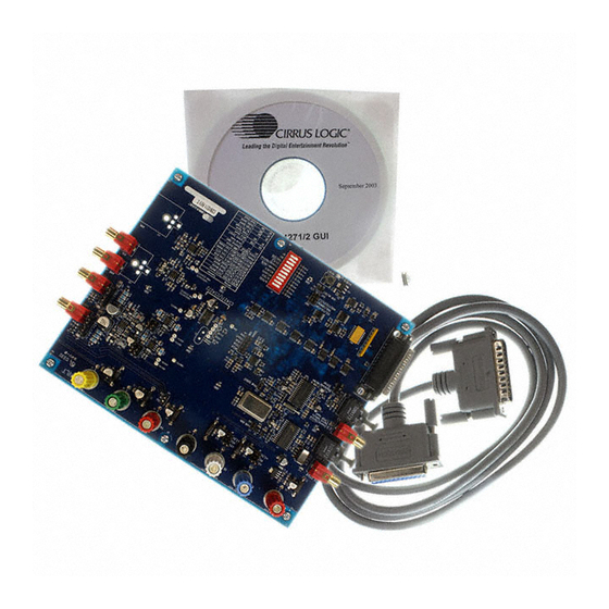
Evaluation Board For CS4271
®
compatible software
Evaluation Board
Control Port
CS4271
Description
The CDB4271 demonstration board is an excellent
means for evaluating the CS4271 stereo CODEC. Eval-
uation requires an analog/digital signal source and
analyzer, and power supplies. Optionally, a Windows
PC compatible computer may be used to evaluate the
CS4271 in control port mode.
System timing can be provided by the CS4271, by the
CS8416 phase-locked to its S/PDIF input, by an I/O
stake header or by an on-board oscillator. RCA phono
jacks are provided for the CS4271 analog outputs and in-
puts. Digital data I/O is available via RCA phono or
optical connectors to the CS8416 and CS8406.
Microsoft Windows
configuration of the board easy. The software communi-
cates through the PC's parallel port to configure the
hardware so that all features of the CS4271 can be eval-
uated. The evaluation board may also be configured to
accept external timing and data signals for operation in a
user application during system development.
SDOUT
MCLK
LRCK
SCLK
SDIN
I/O
Header for
Clocks &
Data
Copyright
Cirrus Logic, Inc. 2003
(All Rights Reserved)
CDB4271
®
software provides a GUI to make
CS8406
S/PDIF
Transmitter
Oscillator
CS8416
S/PDIF
Receiver
®
S/PDIF
Output
S/PDIF
Input
SEPT '03
DS592DB2
1
Advertisement
Table of Contents

Related Manuals for Cirrus Logic CDB4271


Summary of Contents for Cirrus Logic CDB4271
- Page 1 Evaluation Board For CS4271 Features Description Single-ended inputs The CDB4271 demonstration board is an excellent means for evaluating the CS4271 stereo CODEC. Eval- CS8406 S/PDIF digital audio transmitter uation requires an analog/digital signal source and CS8416 S/PDIF digital audio receiver ®...
-
Page 2: Table Of Contents
ANY AND ALL LIABILITY, INCLUDING ATTORNEYS' FEES AND COSTS, THAT MAY RESULT FROM OR ARISE IN CONNECTION WITH THESE USES. Cirrus Logic, Cirrus, and the Cirrus Logic logo designs are trademarks of Cirrus Logic, Inc. All other brand and product names in this document may be trade- marks or service marks of their respective owners. - Page 3 CDB4271 LIST OF FIGURES Figure 1. Instrumentation Amplifier Configuration................6 Figure 2. Main Window ......................... 13 Figure 3. Advanced Window ......................14 Figure 4. I²C Error Message......................14 Figure 5. Clock and Data Routing ....................15 Figure 6. Hierarchy, Schematic Sheet 1 ..................16 Figure 7.
-
Page 4: System Overview
® parallel port interface for use with the supplied Window configuration software. The CDB4271 schematic set has been partitioned into 10 pages and is shown in Figures 6 through 15. CS4271 Stereo Audio CODEC A complete description of the CS4271 is included in the CS4271 product data sheet. -
Page 5: Canned Oscillator
A 1 Vrms single-ended signal will drive the CS4271 inputs to full scale. The CDB4271 was designed for use with not only the CS4271, but also the CS4272 with a simple change of assembly options. For this reason, the input buffer schematic shown in Figure 8 reflects only the configuration assembled on the CDB4271. -
Page 6: Figure 1. Instrumentation Amplifier Configuration
CDB4271 The resistor designated by R2 (see Figure 1) can be adjusted to change the gain of the in- strumentation amp. The feedback resistors ‘R’ on the two sides of the instrumentation amp must be equal. Out+ Out- Figure 1. Instrumentation Amplifier Configuration... -
Page 7: Stand-Alone Control
S1 and its associated logic. PC Parallel Port Control A graphical user interface is included with the CDB4271 to allow easy manipulation of all reg- isters of the CS4271 and hardware configuration of the CDB4271. Connecting a cable to the DB-25 connector (J31) will enable the PC control port, automatically disabling switch S1 and its associated logic. -
Page 8: External Control Headers
CDB4271 External Control Headers The evaluation board has been designed to allow interfacing with external systems via the headers J26, J32, J17, and J24. The 10-pin header, J26, allows the user bidirectional access to MCLK, SCLK, and LRCK. The direction of these signals is set using S1 (see Table 2 for switch control options) or the control port GUI. -
Page 9: Table 1. System Connections
CDB4271 CONNECTOR INPUT/OUTPUT SIGNAL PRESENT +5V - J1 Input +5.0 V Power Supply -18V - J7 Input -18.0 V to -5.0 V Power Supply for the op-amps +18V - J6 Input +5.0 V to +18.0 V Power Supply for the op-amps... -
Page 10: Table 2. Jumper/Switch Settings
CDB4271 JUMPER / SWITCH PURPOSE POSITION FUNCTION SELECTED M/S[1:0] Subclock Master/Slave Select CS4271 is Master (S1) CS8416 is Master CS8406 is Master PCM Header, J26, is Master MCLK[1:0] Master Clock Source Select CS8416 Provides MCLK (S1) CS4271 Provides MCLK PCM Header, J26, Provides MCLK... -
Page 11: Initial Board Setup
4) If desired, create a shortcut to CDB427X.exe on your desktop. You should now be able to run CDB427X.exe. Double-click on CDB427X.exe or its shortcut. 5) Select the LPT port you are using to connect to the CDB4271. 6) Shut down the application, reset the board, and then restart the application. -
Page 12: Verifying Board Operation
CDB4271 2.2.1Verifying Board Operation: 1) If connected, disconnect the PC parallel cable. 2) Set all positions on S1 to LO, with the exception of M0 which should be set to HI. 3) Assert a reset by pressing the RESET button (S2). -
Page 13: Cdb427X.exe User's Guide
427X Main Window The main window of the CDB4271 Graphical User Interface allows the user to view and change the configuration of the CS4271 and on-board configuration logic. The Board Setup box contains all the controls necessary to manage clock and data routing and formats. -
Page 14: Advanced Window
CDB4271 Advanced Window Clicking the “Advanced...” button on the main window will launch a graphical register map of the CS4271. Changes made to the register map will be immediately reflected in the main win- dow, so you may wish to arrange them so that they do not obscure each other. When in I mode, the “Update”... -
Page 15: Block Diagram
CDB4271 4. BLOCK DIAGRAM MCLK LRCK SCLK... -
Page 16: Schematics And Layout
CDB4271 5. SCHEMATICS AND LAYOUT... -
Page 17: Figure 7. Cs4272, Schematic Sheet 2
CDB4271... -
Page 18: Figure 8. Analog Input, Schematic Sheet 3
CDB4271... -
Page 19: Figure 9. Analog Output, Schematic Sheet 4
CDB4271... -
Page 20: Figure 10. Cs8416 S/Pdif Receiver, Schematic Sheet 5
CDB4271... -
Page 21: Figure 11. Cs8406 S/Pdif Transmitter, Schematic Sheet 6
CDB4271... -
Page 22: Figure 12. Board Setup, Schematic Sheet 7
CDB4271... -
Page 23: Figure 13. Pcm Header, Schematic Sheet 8
CDB4271... -
Page 24: Figure 14. Control Port, Schematic Sheet 9
CDB4271... -
Page 25: Figure 15. Power, Schematic Sheet 10
CDB4271... -
Page 26: Figure 16 . Component Placement And Reference Designators
CDB4271... -
Page 27: Figure 17 . Top Layer
CDB4271... -
Page 28: Figure 18 . Bottom Layer
CDB4271... -
Page 29: Appendix
Mouser Electronics Authorized Distributor Click to View Pricing, Inventory, Delivery & Lifecycle Information: Cirrus Logic CDB4271...
Need help?
Do you have a question about the CDB4271 and is the answer not in the manual?
Questions and answers