Table of Contents
Advertisement
Quick Links
Features
Analog Line and Microphone Level Inputs
–
6 RCA and 3 Stereo 1/8" Jacks
–
Compatible with Single-Ended and Pseudo-Diff.
Input Configurations
Analog Line and Headphone Outputs
–
Stereo 1/8" Headphone Jack w/Input Detection
–
4 RCA Jacks for Headphone/Line Outputs
8 to 96 kHz S/PDIF Interface
–
CS8416 Digital Audio Receiver
–
CS8406 Digital Audio Transmitter
I/O Stake Header Accessibility
–
External Control Port Headers
–
External Direct and Buffered Serial Audio I/O
Headers
Multiple Power Supply options via USB, Battery or
External Power Supplies.
1.8 V to 3.3 V Selectable Logic Interface
FlexGUI S/W Control - Windows
–
Pre-Defined & User-Configurable Scripts
USB
USB/
µ controller
RS232
S/PDIF
S/PDIF Tx
Dout
(CS8406)
S/PDIF Rx
S/PDIF
(CS8416)
Din
http://www.cirrus.com
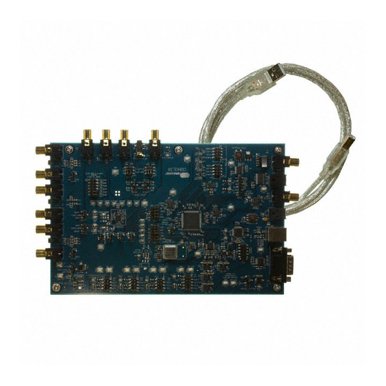
Evaluation Board for CS42L56
®
Compatible
Reset
2
I
C Interface
PLL
Oscillator
(socket)
FPGA
Tx SRC
Rx SRC
(CS8421)
(CS8421)
PSIA I/O Header
Copyright Cirrus Logic, Inc. 2014
Description
The CDB42L56 is the ideal evaluation platform solution to test
and evaluate the CS42L56.The CS42L56 is a highly integrat-
ed, 24-bit, ultra-low power stereo codec based on multi-bit
delta-sigma modulation suitable for low power portable appli-
cations. Use of the board requires an analog/digital signal
source, an analyzer and power supplies. A Windows PC-com-
patible computer is also needed in order to configure the
CS42L56 and the board.
System timing can be provided by the CS8416 (on-board), by
the CS42L56 supplied with a master clock, by the on-board
crystal oscillator or via an I/O stake header with a DSP
connected.
RCA phono connectors and stereo 1/8
provided for CS42L56 analog inputs and HP/Line outputs.
Digital I/O connections are provided via RCA phono or optical
connectors to the CS8416 and CS8406 (S/PDIF Rx and Tx).
The CDB42L56 is programmed via the PC's USB using Cirrus
Logic's Microsoft
evaluation board may also be configured to accept external
timing and data signals for operation in a user application
during system development.
ORDERING INFORMATION
CDB42L56 Evaluation Board
CS42L56
External System
I/O Header
(All Rights Reserved)
CDB42L56
th
inch audio jacks are
®
®
Windows
-based software (FlexGUI). The
Analog Inputs
(Line + MIC)
Analog Outputs
(Line + Headphone)
Reset
FEB '14
DS851DB1
Advertisement
Table of Contents

Related Manuals for Cirrus Logic CDB42L56


Summary of Contents for Cirrus Logic CDB42L56
- Page 1 Evaluation Board for CS42L56 Features Description Analog Line and Microphone Level Inputs The CDB42L56 is the ideal evaluation platform solution to test and evaluate the CS42L56.The CS42L56 is a highly integrat- – 6 RCA and 3 Stereo 1/8” Jacks ed, 24-bit, ultra-low power stereo codec based on multi-bit –...
-
Page 2: Table Of Contents
4.6 Register Maps Tab ......................... 17 5. JUMPER SETTINGS AND SYSTEM CONNECTIONS ................ 18 6. PERFORMANCE PLOTS ........................21 7. CDB42L56 BLOCK DIAGRAM ......................27 8. CDB42L56 SCHEMATICS ........................28 9. CDB42L56 LAYOUT ..........................33 10. REVISION HISTORY .......................... 38 LIST OF FIGURES Figure 1. - Page 3 CDB42L56 Figure 17. Fade-to-Noise Linearity - Analog In to Digital Out ..............22 Figure 18. THD+N vs. Freq. - Digital In to HP Out ..................22 Figure 19. THD+N vs. Amplitude - Digital In to HP Out ................22 Figure 20. THD+N vs. Volume - Digital In to HP Out ................23 Figure 21.
-
Page 4: System Overview
USB. NOTE: The minimum current required for board operation is approximately 300 mA. It may therefore be necessary to connect the CDB42L56 directly to the USB port on the PC as opposed to a hub or keyboard port where the current might be limited. -
Page 5: Cs8421 Sample Rate Converter (Tx Src To Cs42L56)
CDB42L56 Configuration of the CS8416 is made using controls in the “Board Configuration” tab of the Cirrus FlexGUI software. Section 3. “Configuration Options” on page 9 Section 4. “Software Mode Control” on page 11 provide configuration examples and software details. -
Page 6: Oscillator
1.10 Analog Inputs The analog input circuitry on the CDB42L56 has been designed to allow for testing of the CS42L56 in all its possible analog input configurations. Line or microphone level analog input signals can be provided to the analog inputs on the CS42L56 through RCA or microphone input jacks (Figure 35 on page 28). -
Page 7: Analog Outputs
J1 which also allows the user to test the CS42L56’s headphone detect functionality. The CDB42L56 on-board circuitry drives the headphone detect pin low when a headphone is inserted in J1. Headers J12 and J4 can be used to select optional 16 or 32 resistive loads for headphone outputs. -
Page 8: Quick-Start Guide
CDB42L56 2. QUICK-START GUIDE The following figure is a simplified quick-start guide made for user convenience. The guide configures the board with a 1.8 V power supply to VLDO, VA and VCP and a 3.3 V power supply to VL. The user may choose from steps 7 through 10 depending on the desired measurement. -
Page 9: Configuration Options
CDB42L56 3. CONFIGURATION OPTIONS This section shows two common configurations of the CDB42L56. S/PDIF In to Analog Out and Analog In to S/PDIF Out The CS42L56 ADC and DAC performance can be tested by loading the “SPDIF In to Analog Out -- Analog In to S/PDIF Out”... -
Page 10: Psia In To Analog Out And Analog In To Psia Out
CDB42L56 PSIA In to Analog Out and Analog In to PSIA Out The CS42L56 ADC and DAC performance can be tested by loading the “PSIA In to Analog Out -- Analog In to PSIA Out” quick setup file provided with the software package. The script configures the digital clock... -
Page 11: Software Mode Control
Analog Output Volume” and “Register Maps” tabs as desired. 7. Begin evaluating the CS42L56. For quick set-up, the CDB42L56 may, alternatively, be configured by loading a predefined sample script file: 8. On the File menu, click "Restore Board Registers..."... -
Page 12: Board Configuration Tab
CDB42L56 Board Configuration Tab The “Board Configuration” tab provides high-level control of signal routing on the CDB42L56. The controls in this tab are used to setup the CS8416, CS8406, Tx SRC, Rx SRC and the FPGA routing and are divided into separate control groups for each of these individual devices. -
Page 13: Codec Configuration Tab
CDB42L56 Codec Configuration Tab The “Codec Configuration” tab provides high-level control of the CS42L56 register settings. Status text de- tailing the CS42L56’s specific configuration is shown in parenthesis or appears directly below the associat- ed control. This text will change depending on the setting of the associated control. A description of each control group is outlined below. -
Page 14: Codec Analog Input Volume Tab
CDB42L56 Codec Analog Input Volume Tab The “Codec Analog Input Volume” tab provides high-level control of all volume settings in the ADC of the CS42L56. Status text detailing the CS42L56’s specific configuration is shown in parenthesis or inside the control group of the affected control. This text will change depending on the setting of the associated control. -
Page 15: Codec Dsp Engine Tab
CDB42L56 Codec DSP Engine Tab The “Codec DSP Engine” tab provides high-level control functions to modify the SDIN (PCM) data volume level, the ADC output/SDIN mix volume level, the Tone Control and the Beep Generator. Status text detail- ing the CS42L56’s specific configuration is shown inside the control group of the affected control. This text will change depending on the setting of the associated control. -
Page 16: Codec Analog Output Volume Tab
CDB42L56 Codec Analog Output Volume Tab The “Codec Analog Output Volume” tab provides high-level control of the CS42L56 class H output amplifier, HP/Line output volume levels, charge pump frequency, DAC channel limiter, and overall master volume lev- el. A description of each control group is outlined below. -
Page 17: Register Maps Tab
CDB42L56 Register Maps Tab The Register Maps tab provides low-level control of the CS42L56, CS8416, CS8406, CS8421, FPGA and GPIO register settings. Register values can be modified bit-wise or byte-wise. “Left-clicking” on a particular register accesses that register and shows its contents at the bottom. The user can change the register con- tents by using the push-buttons, by selecting a particular bit and typing in the new bit value or by selecting the register in the map and typing in a new hex value. -
Page 18: Jumper Settings And System Connections
CDB42L56 5. JUMPER SETTINGS AND SYSTEM CONNECTIONS CONNECTOR INPUT/OUTPUT SIGNAL PRESENT EXT. +5V Input +5V power supply for evaluation board TP10 Input GND reference from power supply Ext. Input Input +4.5V external power supply for buck converter Input GND reference from power supply Input Socket for +1.5 V AAA batteries for buck converter... -
Page 19: Table 3. Jumper Settings
CDB42L56 LABEL PURPOSE POSITION FUNCTION SELECTED *+1.8V Voltage source is +1.8 V regulator. +2.5V Voltage source is +2.5 V regulator. Selects source of voltage for the +3.3V Voltage source is +3.3 V regulator. VL supply +1.8VB Voltage source is +1.8 V from battery. - Page 20 CDB42L56 *2 - 4, *1 - 3 Unfiltered output selected for HPOUTA. Selects filtered or unfiltered output HPOUTA FLT/NOFLT for HPOUTA 4 - 6, 3 - 5 RC filtered output selected for HPOUTA. *2 - 4, *1 - 3 Unfiltered output selected for HPOUTB.
-
Page 21: Performance Plots
CDB42L56 6. PERFORMANCE PLOTS Test conditions (unless otherwise specified): T = 25°C; VA=VCP=VLDO=VL=1.8 V; input test signal is a full-scale 997 Hz sine wave; dB values relative to full-scale output; measurement bandwidth 20 Hz to 20 kHz (un-weighted); Sample Frequency = 48 kHz; +2 dB analog gain for Line Output path; -4 dB analog gain for Headphone Output path;... -
Page 22: Figure 14. Fft - Analog In To Digital Out - No Input
CDB42L56 -100 -100 -110 -110 -120 -120 -130 -130 -140 -140 Figure 15. Figure 14. FFT - Analog In to Digital Out - No Input FFT Crosstalk - Analog In to Digital Out @ -1 dBFS TTT T +4.5 +3.5 +2.5... -
Page 23: Figure 20. Thd+N Vs. Volume - Digital In To Hp Out
CDB42L56 Master Volume (Digital) -100 -100 Headphone Volume -110 -102 -104 (Analog) -120 -106 -130 -108 -110 -140 dBr A Figure 21. Figure 20. THD+N vs. Volume - Digital In to HP Out FFT - Digital In to HP Out @ 0 dBFS... -
Page 24: Figure 24. Freq. Response - Digital In To Hp Out
CDB42L56 +4.5 +3.5 +2.5 +1.5 +0.5 -0.5 -1.5 -2.5 -3.5 -4.5 -140 -120 -100 dBFS Figure 24. Figure 25. Freq. Response - Digital In to HP Out Fade-to-Noise Linearity- Digital In to HP Out -100 -100 -120 -100 dBFS Figure 27. -
Page 25: Figure 28. Thd+N Vs. Volume - Digital In To Line Out
CDB42L56 Master Volume (Digital) -100 Line Volume -100 -110 -102 (Analog) -120 -104 -106 -130 -108 -140 -110 dBr A Figure 28. THD+N vs. Volume - Digital In to Line Out Figure 29. FFT Crosstalk - Digital In to Line Out @ 0 dBFS... -
Page 26: Figure 32. Freq. Response - Digital In To Line Out
CDB42L56 +4.5 +3.5 +2.5 +1.5 +0.5 -0.5 -1.5 -2.5 -3.5 -4.5 -140 -120 -100 dBFS Figure 32. Figure 33. Freq. Response - Digital In to Line Out Fade-to-Noise Linearity- Digital In to Line Out DS851DB1... -
Page 27: Cdb42L56 Block Diagram
7. CDB42L56 BLOCK DIAGRAM Reset USB/ µ controller C Interface RS232 Oscillator (socket) S/PDIF S/PDIF Tx Analog Inputs Dout (CS8406) (Line + MIC) CS42L56 FPGA Analog Outputs S/PDIF Rx S/PDIF (Line + Headphone) (CS8416) Reset Tx SRC Rx SRC (CS8421) -
Page 28: Cdb42L56 Schematics
8. CDB42L56 SCHEMATICS Figure 35. CS42L56 & Analog I/O (Schematic Sheet 1) -
Page 29: Figure 36. S/Pdif & Digital Interface (Schematic Sheet 2)
Figure 36. S/PDIF & Digital Interface (Schematic Sheet 2) -
Page 30: Figure 37. Pll, Oscillator And External I/O Connections (Schematic Sheet 3)
Figure 37. PLL, oscillator and external I/O connections (Schematic Sheet 3) -
Page 31: Figure 38. Microcontroller And Fpga (Schematic Sheet 4)
Figure 38. Microcontroller and FPGA (Schematic Sheet 4) -
Page 32: Figure 39. Power (Schematic Sheet 5)
Figure 39. Power (Schematic Sheet 5) -
Page 33: Cdb42L56 Layout
9. CDB42L56 LAYOUT Figure 40. Silk Screen... -
Page 34: Figure 41. Top-Side Layer
Figure 41. Top-Side Layer... -
Page 35: Figure 42. Gnd (Layer 2)
Figure 42. GND (Layer 2) -
Page 36: Figure 43. Power (Layer 3)
Figure 43. Power (Layer 3) -
Page 37: Figure 44. Bottom Side Layer
Figure 44. Bottom Side Layer... -
Page 38: Revision History
LIABILITY, INCLUDING ATTORNEYS’ FEES AND COSTS, THAT MAY RESULT FROM OR ARISE IN CONNECTION WITH THESE USES. Cirrus Logic, Cirrus, and the Cirrus Logic logo designs are trademarks of Cirrus Logic, Inc. All other brand and product names in this document may be trademarks or service marks of their respective owners.
Need help?
Do you have a question about the CDB42L56 and is the answer not in the manual?
Questions and answers