Table of Contents
Advertisement
Quick Links
Download this manual
See also:
Reference Manual
Advertisement
Table of Contents

Related Manuals for Altera Arria II GX


Summary of Contents for Altera Arria II GX
- Page 1 Arria II GX FPGA Development Board, 6G Edition Reference Manual 101 Innovation Drive Document Version: San Jose, CA 95134 Document Date: July 2010 www.altera.com...
- Page 2 Altera warrants performance of its semiconductor products to current specifications in accordance with Altera's standard warranty, but reserves the right to make changes to any products and services at any time without notice. Altera assumes no responsibility or liability arising out of the application or use of any information, product, or service described herein except as expressly agreed to in writing by Altera Corporation.
-
Page 3: Table Of Contents
Featured Device: Arria II GX Device ........ - Page 4 How to Contact Altera ........
-
Page 5: Chapter 1. Overview
Design advancements and innovations, such as the 6.375-Gbps transceiver modules, the PCI Express hard IP implementation, and programmable power technology ensure that designs implemented in the Arria II GX FPGAs operate faster, with lower power, and have a faster time to market than previous FPGA families. -
Page 6: Board Component Blocks
1–2 Chapter 1: Overview Board Component Blocks Board Component Blocks The board features the following major component blocks: Arria II GX EP2AGX260FF35 FPGA in the 1152-pin FineLine BGA (FBGA) package ■ 244,188 LEs ■ 102,600 adaptive logic modules (ALMs) ■... - Page 7 PCI Express edge connector power ■ On-board power measurement circuitry ■ Mechanical ■ PCI Express full-length standard-height (8.48” x 4.376”) ■ PCI Express chassis or bench-top operation ■ © July 2010 Altera Corporation Arria II GX FPGA Development Board, 6G Edition Reference Manual...
-
Page 8: Development Board Block Diagram
Chapter 1: Overview Development Board Block Diagram Development Board Block Diagram Figure 1–1 shows the block diagram of the Arria II GX FPGA development board, 6G Edition. Figure 1–1. Arria II GX FPGA Development Board, 6G Edition Block Diagram Port A... -
Page 9: Introduction
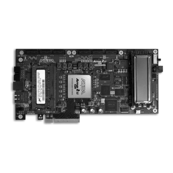
■ “Statement of China-RoHS Compliance” on page 2–52 Board Overview This section provides an overview of the Arria II GX FPGA development board, 6G Edition, including an annotated board image and component descriptions. Figure 2–1 provides an overview of the development board features. - Page 10 Controller (J14) (D24-D26) (U32) Table 2–1 describes the components and lists their corresponding board references. Table 2–1. Arria II GX FPGA Development Board, 6G Edition Components (Part 1 of 3) Board Reference Type Description Featured Devices FPGA EP2AGX260FF35, 1152-pin FBGA.
- Page 11 Chapter 2: Board Components 2–3 Board Overview Table 2–1. Arria II GX FPGA Development Board, 6G Edition Components (Part 2 of 3) Board Reference Type Description D11, D12, D13 Configuration LEDs Illuminates to show the LED sequence that determines which flash memory image loads to the FPGA when LOAD IMAGE is pressed.
-
Page 12: Featured Device: Arria Ii Gx Device
2–4 Chapter 2: Board Components Featured Device: Arria II GX Device Table 2–1. Arria II GX FPGA Development Board, 6G Edition Components (Part 3 of 3) Board Reference Type Description Memory Devices DDR2 SODIMM DDR2 x64 SODIMM 200-pin connector and is populated with a 1-Gbyte memory module. -
Page 13: I/O Resources
Transceivers Package Type 102,600 244,188 11,756 1152-pin FBGA Table 2–3 lists the Arria II GX component reference and manufacturing information. Table 2–3. Arria II GX Device Component Reference and Manufacturing Information Manufacturing Manufacturer Board Reference Description Manufacturer Part Number Website... -
Page 14: Max Ii Cpld Epm2210 System Controller
Note to Table 2–4: (1) Transceiver signals are not included. Table 2–5 lists the Arria II GX device pin count and usage by function on the development board. Table 2–5. Arria II GX Device Pin Count and Usage Function I/O Standard... - Page 15 Programmable oscillator 2 output divider 0 clk2_od[0] 2.5-V — Programmable oscillator 2 output divider 1 clk2_od[1] 2.5-V — Programmable oscillator 2 output divider 2 clk2_od[2] © July 2010 Altera Corporation Arria II GX FPGA Development Board, 6G Edition Reference Manual...
- Page 16 FPGA configuration data fpga_config_d[7] 2.5-V FPGA configuration clock fpga_dclk 2.5-V AC26 FPGA configuration active fpga_nconfig 2.5-V AD28 FPGA configuration ready fpga_nstatus 2.5-V FSM bus address fsm_a[0] Arria II GX FPGA Development Board, 6G Edition Reference Manual © July 2010 Altera Corporation...
- Page 17 2.5-V FSM bus data fsm_d[17] 2.5-V FSM bus data fsm_d[18] 2.5-V FSM bus data fsm_d[19] 2.5-V FSM bus data fsm_d[2] 2.5-V FSM bus data fsm_d[20] © July 2010 Altera Corporation Arria II GX FPGA Development Board, 6G Edition Reference Manual...
- Page 18 2.5-V FSM bus Max2 byte enable 1 max2_ben[1] 2.5-V FSM bus Max2 byte enable 2 max2_ben[2] 2.5-V FSM bus Max2 byte enable 3 max2_ben[3] Arria II GX FPGA Development Board, 6G Edition Reference Manual © July 2010 Altera Corporation...
-
Page 19: Configuration, Status, And Setup Elements
The USB-Blaster is implemented using a USB Type-B connector (J6), a FTDI USB 2.0 PHY device (U15), and an Altera MAX II CPLD (U32). This allows the configuration of the FPGA using a USB cable directly connected between the USB port on the board (J6) and a USB port of a PC running the Quartus II software. - Page 20 GUI interfaces. For this setting, remove the left-most jumper shunt from the JTAG chain header (J9). Flash Memory Programming Flash memory programming is possible through a variety of methods using the Arria II GX device. Arria II GX FPGA Development Board, 6G Edition Reference Manual © July 2010 Altera Corporation...
-
Page 21: Fpga Programming From Flash Memory
The PFL megafunction is a block of logic that is programmed into an Altera programmable logic device (FPGA or CPLD). The PFL functions as a utility for writing to a compatible flash memory device. This... - Page 22 FLASH_CLK FLASH_RSTn CONFIG_LED1 CONFIG_LED2 MSEL [3:0] 10 kΩ 2.5 V Flash FLASH_A [25:1] 10 kΩ FLASH_D [15:0] FLASH_CEn FLASH_OEn FLASH_WEn FLASH_ADVn FLASH_CLK FLASH_RSTn FLASH_RSTn FLASH_RYBSYn Arria II GX FPGA Development Board, 6G Edition Reference Manual © July 2010 Altera Corporation...
- Page 23 CONFIG[2:0] LED (D11, D12, D13) is illuminated. Table 2–9 defines the hardware page that loads when the load image push-button switch (PB5) is pressed. © July 2010 Altera Corporation Arria II GX FPGA Development Board, 6G Edition Reference Manual...
-
Page 24: Fpga Programming Over External Usb-Blaster
Green LED. Illuminates to indicate Ethernet PHY transmit activity. Driven by the Marvell 88E1111 PHY. ENET RX Green LED. Illuminates to indicate Ethernet PHY receive activity. Driven by the Marvell 88E1111 PHY. Arria II GX FPGA Development Board, 6G Edition Reference Manual © July 2010 Altera Corporation... -
Page 25: Setup Elements
Table 2–12. Board Settings DIP Switch Controls (Part 1 of 2) Switch Schematic Signal Name Description Default Reserved MAX_DIP0 Reserved MAX_DIP1 © July 2010 Altera Corporation Arria II GX FPGA Development Board, 6G Edition Reference Manual... -
Page 26: Jtag Chain Header Switch
JTAG Chain Header Switch The JTAG chain header switch (J9) is provided to either remove or include devices in the active JTAG chain. However, the Arria II GX FPGA device is always in the JTAG chain. Table 2–14 shows the switch controls and its descriptions. -
Page 27: Pci Express Control Dip Switch
LED_CONFIG_LED[2:0] sequence. Refer to Table 2–9 for the LED_CONFIG_LED[2:0] sequence definitions. The MAX II reset push-button switch, MAX_RESETn (PB4), resets the MAX II CPLD EPM2210 System Controller. © July 2010 Altera Corporation Arria II GX FPGA Development Board, 6G Edition Reference Manual... -
Page 28: Clock Circuitry
The development board has two types of clock inputs: global clock inputs and transceiver reference clock inputs. Figure 2–6 shows the Arria II GX FPGA development board, 6G Edition clock inputs. Figure 2–6. Arria II GX FPGA Development Board, 6G Edition Clock Inputs 7 6 5 4 3 2 1 0... - Page 29 Chapter 2: Board Components 2–21 Clock Circuitry Table 2–19 shows the external clock inputs for the Arria II GX FPGA development board, 6G Edition. Table 2–19. Arria II GX FPGA Development Board, 6G Edition Clock Inputs Source Schematic Signal Name...
-
Page 30: Arria Ii Gx Fpga Clock Outputs
HSMB_CLKOUT0 (2.5 V) PLL 1 PLL 4 Table 2–20 lists the clock outputs for the Arria II GX FPGA development board, 6G Edition. Table 2–20. Arria II GX FPGA Development Board, 6G Edition Clock Outputs Connector Schematic Signal Name I/O Standard Description 2.5-V... -
Page 31: General User Input/Output
The board reference PB3 is the CPU reset push-button switch, CPU_RESET, which is an input to the Arria II GX device. CPU_RESET is intended to be the master reset signal for the FPGA design loaded into the Arria II GX device. It also acts as a regular I/O pin. -
Page 32: User-Defined Dip Switches
LEDs from the FPGA designs loaded into the Arria II GX device. The LEDs illuminate when a logic 0 is driven, and turns off when a logic 1 is driven. There is no board-specific function for these LEDs. -
Page 33: Hsmc User-Defined Leds
Labeled RX for HSMC port A. 2.5-V User-defined LEDs. AE24 HSMB_TX_LED Labeled TX for HSMC port B. User-defined LEDs. AF23 HSMB_RX_LED Labeled RX for HSMC port B. © July 2010 Altera Corporation Arria II GX FPGA Development Board, 6G Edition Reference Manual... -
Page 34: Lcd
Table 2–31. LCD Pin Definitions and Functions (Part 1 of 2) Number Symbol Level Function — Power supply — GND (0 V) — For LCD drive Arria II GX FPGA Development Board, 6G Edition Reference Manual © July 2010 Altera Corporation... -
Page 35: Components And Interfaces
HSMC PCI Express The Arria II GX FPGA development board, 6G Edition is designed to fit entirely into a PC motherboard with a ×8 PCI Express slot that can accommodate a full height long form factor add-in card. This interface uses the Arria II GX device's PCI Express hard IP block, saving logic resources for the user logic application. - Page 36 This signal is connected directly to a Arria II GX REFCLK input pin pair using DC coupling. This clock is terminated on the motherboard and therefore, no on-board termination is required.
- Page 37 PCIE_WAKEn J14.B5 SMB clock PCIE_SMBCLK J14.B6 SMB data LVTTL PCIE_SMBDAT — x1 Presence detect PCIE_LED_X1 — x4 Presence detect PCIE_LED_X4 — x8 Presence detect PCIE_LED_X8 © July 2010 Altera Corporation Arria II GX FPGA Development Board, 6G Edition Reference Manual...
-
Page 38: 10/100/1000 Ethernet
U24.11 RGMII transmit data ENET_TXD[0] U24.12 RGMII transmit data ENET_TXD[1] U24.14 RGMII transmit data ENET_TXD[2] U24.16 RGMII transmit data ENET_TXD[3] U24.9 RGMII transmit control ENET_TX_EN Arria II GX FPGA Development Board, 6G Edition Reference Manual © July 2010 Altera Corporation... -
Page 39: High-Speed Mezzanine Cards
The development board contains two HSMC interfaces called port A and port B. The HSMC port B is only available in the Arria II GX FPGA development board, 6G Edition. HSMC port A interface supports both single-ended and differential signaling while HSMC port B interface only supports single-ended signaling. - Page 40 Dedicated CMOS I/O bit 0 HSMA_D0 J2.42 Dedicated CMOS I/O bit 1 HSMA_D1 J2.43 Dedicated CMOS I/O bit 2 HSMA_D2 J2.44 Dedicated CMOS I/O bit 3 HSMA_D3 Arria II GX FPGA Development Board, 6G Edition Reference Manual © July 2010 Altera Corporation...
- Page 41 LVDS or CMOS clock in 1 or CMOS bit 39 HSMA_CLKIN_N1 J2.101 LVDS TX bit 8 or CMOS bit 40 HSMA_TX_D_P8 J2.102 LVDS RX bit 8 or CMOS bit 41 HSMA_RX_D_P8 © July 2010 Altera Corporation Arria II GX FPGA Development Board, 6G Edition Reference Manual...
- Page 42 HSMA_CLKIN_P2 J2.157 LVDS or CMOS clock out 2 or CMOS bit 78 HSMA_CLKOUT_N2 J2.158 LVDS or CMOS clock in 2 or CMOS bit 79 HSMA_CLKIN_N2 Arria II GX FPGA Development Board, 6G Edition Reference Manual © July 2010 Altera Corporation...
- Page 43 HSMB_CLKIN0 J1.41 Dedicated CMOS I/O bit 0 AH29 HSMB_D0 J1.42 Dedicated CMOS I/O bit 1 AH30 HSMB_D1 J1.43 Dedicated CMOS I/O bit 2 AK30 HSMB_D2 © July 2010 Altera Corporation Arria II GX FPGA Development Board, 6G Edition Reference Manual...
- Page 44 Dedicated CMOS I/O bit 37 AD10 HSMB_D37 J1.97 Dedicated CMOS I/O bit 38 HSMB_D38 J1.98 Dedicated CMOS I/O bit 39 HSMB_D39 J1.101 Dedicated CMOS I/O bit 40 HSMB_D40 Arria II GX FPGA Development Board, 6G Edition Reference Manual © July 2010 Altera Corporation...
- Page 45 LVDS or CMOS clock out 2 or CMOS bit 76 HSMB_CLKOUT_P2 J1.156 Dedicated CMOS I/O bit 74 HSMB_D74 J1.157 LVDS or CMOS clock out 2 or CMOS bit 77 HSMB_CLKOUT_N2 © July 2010 Altera Corporation Arria II GX FPGA Development Board, 6G Edition Reference Manual...
-
Page 46: Memory
ASP-122953-01 www.samtec.com family high-speed socket. Memory This section describes the board's memory interface support and also their signal names, types, and connectivity relative to the Arria II GX device. The board has the following memory interfaces: ■ DDR3 DDR2 SODIMM ■... - Page 47 U13.J3 Row address select DDR3_RAS_n U13.T2 Reset DDR3_RST_n U13.L3 Write enable DDR3_WE_n U13.J7 Clock P DDR3_CLK_P Differential 1.5-V SSTL Class I U13.K7 Clock N DDR3_CLK_N © July 2010 Altera Corporation Arria II GX FPGA Development Board, 6G Edition Reference Manual...
-
Page 48: Ddr2 Sodimm
DDR2 SODIMM pin assignments, signal names, and its functions. The signal names and types are relative to the Arria II device in terms of I/O setting and direction. Arria II GX FPGA Development Board, 6G Edition Reference Manual © July 2010 Altera Corporation... - Page 49 J7.109 Write enable DDR2_WE_n J7.30 Clock P0 DDR2_CLK_P0 J7.32 Clock N0 DDR2_CLK_N0 Differential 1.8-V SSTL Class I J7.164 Clock P1 DDR2_CLK_P1 J7.166 Clock N1 DDR2_CLK_N1 © July 2010 Altera Corporation Arria II GX FPGA Development Board, 6G Edition Reference Manual...
- Page 50 DDR2_DQ25 J7.73 Data bus byte lane 3 AE18 DDR2_DQ26 J7.75 Data bus byte lane 3 AP18 DDR2_DQ27 J7.62 Data bus byte lane 3 AH19 DDR2_DQ28 Arria II GX FPGA Development Board, 6G Edition Reference Manual © July 2010 Altera Corporation...
- Page 51 J7.176 Data bus byte lane 6 AL11 DDR2_DQ55 J7.170 Write mask byte lane 6 AC15 DDR2_DM6 J7.169 Data strobe P byte lane 6 AK13 DDR2_DQS6 © July 2010 Altera Corporation Arria II GX FPGA Development Board, 6G Edition Reference Manual...
-
Page 52: Ssram
Table 2–43 lists the SSRAM pin assignments, signal names, and functions. The signal names and types are relative to the Arria II GX device in terms of I/O setting and direction. Arria II GX FPGA Development Board, 6G Edition Reference Manual... - Page 53 FSM_D10 U22.E11 Data bus FSM_D11 U22.F10 Data bus FSM_D12 U22.F11 Data bus FSM_D13 U22.G10 Data bus FSM_D14 U22.G11 Data bus FSM_D15 U22.D1 Data bus FSM_D16 © July 2010 Altera Corporation Arria II GX FPGA Development Board, 6G Edition Reference Manual...
- Page 54 U22.B7 Global write enable SRAM_GWn U22.R1 Mode — SRAM_MODE (Connects to the MAX II CPLD EPM2210 System Controller) U22.B8 Output enable SRAM_OEn U22.H11 Sleep SRAM_ZZ Arria II GX FPGA Development Board, 6G Edition Reference Manual © July 2010 Altera Corporation...
-
Page 55: Flash
Table 2–45 lists the flash pin assignments, signal names, and functions. The signal names and types are relative to the Arria II GX device in terms of I/O setting and direction. Table 2–45. Flash Pin Assignments, Schematic Signal Names, and Functions (Part 1 of 2) - Page 56 Table 2–46. Flash Component Reference and Manufacturing Information Manufacturing Manufacturer Board Reference Description Manufacturer Part Number Website 512 Mbyte Synchronous Flash Numonyx PC28F512P30BF www.numonyx.com Arria II GX FPGA Development Board, 6G Edition Reference Manual © July 2010 Altera Corporation...
-
Page 57: Power Supply
Regulator inefficiencies and sharing are reflected in the currents shown, which are conservative absolute maximum levels. © July 2010 Altera Corporation Arria II GX FPGA Development Board, 6G Edition Reference Manual... - Page 58 (2.243 A no HSMCs) TPS71725 3.0 A Maximum 0.143 A 0.091 A A2GX GXB PMA SENSE A2VCCA PLL 2.5 V 0.052 A A2GX Analog PLL BEAD Arria II GX FPGA Development Board, 6G Edition Reference Manual © July 2010 Altera Corporation...
-
Page 59: Power Measurement
ADC to measure voltage and current. An SPI bus connects these ADC devices to the MAX II CPLD EPM2210 System Controller as well as the Arria II GX FPGA. Figure 2–12 shows the block diagram for the power measurement circuitry. -
Page 60: Statement Of China-Rohs Compliance
(2) X* indicates that the concentration of the hazardous substance of at least one of all homogeneous materials in the parts is above the relevant threshold of the SJ/T11363-2006 standard, but it is exempted by EU RoHS. Arria II GX FPGA Development Board, 6G Edition Reference Manual © July 2010 Altera Corporation... -
Page 61: Revision History
Non-technical support (General) Email nacomp@altera.com (Software Licensing) Email authorization@altera.com Note to Table: (1) You can also contact your local Altera sales office or sales representative. © July 2010 Altera Corporation Arria II GX FPGA Development Board, 6G Edition Preliminary... -
Page 62: Typographic Conventions
A warning calls attention to a condition or possible situation that can cause you injury. The angled arrow instructs you to press Enter. The feet direct you to more information about a particular topic. Arria II GX FPGA Development Board, 6G Edition © July 2010 Altera Corporation Preliminary...
Need help?
Do you have a question about the Arria II GX and is the answer not in the manual?
Questions and answers