
Related Manuals for Altera Stratix IV E FPGA


Summary of Contents for Altera Stratix IV E FPGA
- Page 1 Stratix IV E FPGA Development Board Reference Manual Stratix IV E FPGA Development Board Reference Manual 101 Innovation Drive San Jose, CA 95134 www.altera.com MNL-01048-1.2 Subscribe Arrow.com. Downloaded from...
- Page 2 © 2011 Altera Corporation. All rights reserved. ALTERA, ARRIA, CYCLONE, HARDCOPY, MAX, MEGACORE, NIOS, QUARTUS and STRATIX are Reg. U.S. Pat. & Tm. Off. and/or trademarks of Altera Corporation in the U.S. and other countries. All other trademarks and service marks are the property of their respective holders as described at www.altera.com/common/legal.html.
-
Page 3: Table Of Contents
Stratix IV E FPGA Clocks ........ - Page 4 How to Contact Altera ........
-
Page 5: Chapter 1. Overview
The Stratix IV E FPGA development board provides a hardware platform for developing and prototyping high-performance and logic-intensive designs based on Altera Stratix IV E devices. The board provides a wide range of peripherals and memory interfaces to facilitate the development of the Stratix IV E FPGA designs. - Page 6 125-MHz oscillator (two differential inputs to the FPGA) ■ SMA connectors for external clock input ■ SMA connector for clock output ■ HSMC input and output ports ■ Stratix IV E FPGA Development Board Reference Manual May 2011 Altera Corporation Arrow.com. Arrow.com. Arrow.com. Arrow.com. Arrow.com. Arrow.com.
- Page 7 ■ 20-W per HSMC interface ■ ■ Mechanical 8.25” x 7” board ■ Bench-top operation ■ May 2011 Altera Corporation Stratix IV E FPGA Development Board Reference Manual Arrow.com. Arrow.com. Arrow.com. Arrow.com. Arrow.com. Arrow.com. Arrow.com. Downloaded from Downloaded from Downloaded from...
-
Page 8: Development Board Block Diagram
Chapter 1: Overview Development Board Block Diagram Development Board Block Diagram Figure 1–1 shows the block diagram of the Stratix IV E FPGA development board. Figure 1–1. Stratix IV E FPGA Development Board Block Diagram 2 GB DDR3 SDRAM DIMM (x72) Power... -
Page 9: Introduction
2. Board Components Introduction This chapter introduces the major components on the Stratix IV E FPGA development board. Figure 2–1 illustrates major component locations and Table 2–1 provides a brief description of all component features of the board. A complete set of schematics, a physical layout database, and GERBER files for the development board reside in the Stratix IV E FPGA development kit documents directory. -
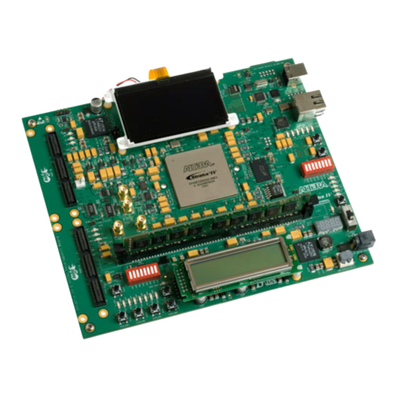
Page 10: Board Overview
2–2 Chapter 2: Board Components Board Overview Board Overview This section provides an overview of the Stratix IV E FPGA development board, including an annotated board image and component descriptions. Figure 2–1 provides an overview of the development board features. - Page 11 Chapter 2: Board Components 2–3 Board Overview Table 2–1. Stratix IV E FPGA Development Board Components (Part 2 of 4) Board Reference Type Description Place a shunt on this header to include the HSMC port A in the JTAG HSMC Port A JTAG header chain.
- Page 12 2–4 Chapter 2: Board Components Board Overview Table 2–1. Stratix IV E FPGA Development Board Components (Part 3 of 4) Board Reference Type Description CLKIN_P SMA (positive) Drives LVPECL-compatible differential clock inputs into the LVDS clock buffer (U22).The CLK66_SEL signal needs to be set to '1' on SW2 to enable the SMA clock source.
-
Page 13: Featured Device: Stratix Iv E Device
Chapter 2: Board Components 2–5 Featured Device: Stratix IV E Device Table 2–1. Stratix IV E FPGA Development Board Components (Part 4 of 4) Board Reference Type Description A single 250-MHz 18-Mb (2 M x 36) SSRAM device with a 165-BGA SSRAM x36 memory package footprint. -
Page 14: I/O Resources
Seven-Segment Display 2.5-V CMOS — EEPROM 2.5-V CMOS — MAX II Control, Speaker 2.5-V CMOS — Device I/O Total: Stratix IV E FPGA Development Board Reference Manual May 2011 Altera Corporation Arrow.com. Arrow.com. Arrow.com. Arrow.com. Arrow.com. Arrow.com. Arrow.com. Arrow.com. Arrow.com. -
Page 15: Max Ii Cpld Epm2210 System Controller
Chapter 2: Board Components 2–7 MAX II CPLD EPM2210 System Controller MAX II CPLD EPM2210 System Controller The board utilizes the EPM2210 System Controller, an Altera MAX II CPLD, for the following purposes: ■ FPGA configuration from flash memory ■... - Page 16 U3.A2, U2.D1 FSM bus address FSM_A4 2.5-V U3.A10, U2.D2 FSM bus address FSM_A5 2.5-V U3.B2, U2.A2 FSM bus address FSM_A6 Stratix IV E FPGA Development Board Reference Manual May 2011 Altera Corporation Arrow.com. Arrow.com. Arrow.com. Arrow.com. Arrow.com. Arrow.com. Arrow.com. Arrow.com.
- Page 17 U3.G11, U2.E7 FSM bus data FSM_D15 2.5-V U3.D1 FSM bus data FSM_D16 2.5-V U3.D2 FSM bus data FSM_D17 May 2011 Altera Corporation Stratix IV E FPGA Development Board Reference Manual Arrow.com. Arrow.com. Arrow.com. Arrow.com. Arrow.com. Arrow.com. Arrow.com. Arrow.com. Arrow.com. Arrow.com.
- Page 18 MAX_OEn 2.5-V — FSM bus MAX II output enable User-defined push-button switch MAX_PB 2.5-V — (labeled as USER_2 on the board) Stratix IV E FPGA Development Board Reference Manual May 2011 Altera Corporation Arrow.com. Arrow.com. Arrow.com. Arrow.com. Arrow.com. Arrow.com. Arrow.com.
- Page 19 Temperature monitor SMB clock TSENSE_SMB_DATA 2.5-V — U18.12, U21.7 Temperature monitor SMB data VDDQ_QDRII_PG 2.5-V — U16.7 I/O supply May 2011 Altera Corporation Stratix IV E FPGA Development Board Reference Manual Arrow.com. Arrow.com. Arrow.com. Arrow.com. Arrow.com. Arrow.com. Arrow.com. Arrow.com. Arrow.com. Arrow.com. Arrow.com.
-
Page 20: Configuration, Status, And Setup Elements
The USB-Blaster is implemented using a USB Type-B connector (J6), a FTDI USB 2.0 PHY device (U7), and an Altera MAX II CPLD (U10). This allows the configuration of the FPGA using a USB cable directly connected between the USB port on the board (J6) and a USB port of a PC running the Quartus II software. - Page 21 The MAX II CPLD EPM2210 System Controller must be in the chain to use some of the GUI interfaces. For this setting, place a jumper shunt on the MAX II JTAG header (J10). May 2011 Altera Corporation Stratix IV E FPGA Development Board Reference Manual Arrow.com. Arrow.com. Arrow.com.
-
Page 22: Flash Memory Programming
The PFL megafunction is a block of logic that is programmed into an Altera programmable logic device (FPGA or CPLD). The PFL functions as a utility for writing to a compatible flash memory device. This... -
Page 23: Status Elements
■ II Software. Status Elements The development board includes general user, board specific, and status LEDs. This section describes the status elements. May 2011 Altera Corporation Stratix IV E FPGA Development Board Reference Manual Arrow.com. Arrow.com. Arrow.com. Arrow.com. Arrow.com. Arrow.com. - Page 24 AH29 U10.E3 FPGA_CONF_DONE MAX II CPLD EPM2210 System Controller. Blue LED. Illuminates when 12-V power rail — — — is active. Stratix IV E FPGA Development Board Reference Manual May 2011 Altera Corporation Arrow.com. Arrow.com. Arrow.com. Arrow.com. Arrow.com. Arrow.com. Arrow.com.
-
Page 25: Setup Elements
Clock enable DIP switch JTAG chain jumpers ■ ■ On-Board memory headers ■ Reset configuration push-button switch ■ Rotary switch May 2011 Altera Corporation Stratix IV E FPGA Development Board Reference Manual Arrow.com. Arrow.com. Arrow.com. Arrow.com. Arrow.com. Arrow.com. Arrow.com. Arrow.com. Arrow.com. -
Page 26: Max Ii Dip Switch
Table 2–11. MAX II DIP Switch Component Reference and Manufacturing Information Manufacturer Board Reference Description Manufacturer Manufacturer Website Part Number Eight-Position slide DIP switch Grayhill 76SB08ST www.grayhill.com Stratix IV E FPGA Development Board Reference Manual May 2011 Altera Corporation Arrow.com. Arrow.com. Arrow.com. Arrow.com. Arrow.com. Arrow.com. Arrow.com. Arrow.com. Arrow.com. -
Page 27: User Dip Switch
ENABLE CLK100_EN switch is in the CLOSED or DISABLE position, a logic 0 is selected. — U10.J2 ENABLE CLK125_EN May 2011 Altera Corporation Stratix IV E FPGA Development Board Reference Manual Arrow.com. Arrow.com. Arrow.com. Arrow.com. Arrow.com. Arrow.com. Arrow.com. Arrow.com. Arrow.com. -
Page 28: Jtag Chain Jumpers
JTAG Chain Jumpers The JTAG chain jumpers are provided to either remove or include devices in the active JTAG chain. However, the Stratix IV E FPGA device is always in the JTAG chain. Table 2–16 shows the jumper controls and its descriptions. -
Page 29: On-Board Memory Headers
Board Manufacturer Description Manufacturer Manufacturer Website Reference Part Number www.panasonic.com/industrial/components/ Push-Button switch Panasonic EVQPAC07K components.html May 2011 Altera Corporation Stratix IV E FPGA Development Board Reference Manual Arrow.com. Arrow.com. Arrow.com. Arrow.com. Arrow.com. Arrow.com. Arrow.com. Arrow.com. Arrow.com. Arrow.com. Arrow.com. Arrow.com. Arrow.com. -
Page 30: Rotary Switch
94HCB16WT www.grayhill.com Clock Circuitry This section describes the board's clocking circuitry. Stratix IV E FPGA Clocks The development board has several on-board oscillators. Stratix IV E FPGA Development Board Reference Manual May 2011 Altera Corporation Arrow.com. Arrow.com. Arrow.com. Arrow.com. Arrow.com. - Page 31 EP4SE530H35 CLKIN_SMA Table 2–22 shows the clock distribution for the Stratix IV E FPGA development board. Table 2–22. Stratix IV E FPGA Development Board Clock Distribution (Part 1 of 2) Frequency Schematic Signal Name Signal Originates From Signal Propagates To CLKIN_66M_P0 U19.W33...
-
Page 32: General User Input/Output
2–24 Chapter 2: Board Components General User Input/Output Table 2–22. Stratix IV E FPGA Development Board Clock Distribution (Part 2 of 2) Frequency Schematic Signal Name Signal Originates From Signal Propagates To 50 MHz CLKIN_50 X5.3 U19.V33 and U10.J12 6.000 MHz USB_XTAL U7.27 and U7.28 (USB PHY, FT245BL) -
Page 33: User-Defined Leds
The board reference S4 is the CPU reset push-button switch, CPU_RESETn, which is an input to the Stratix IV E FPGA device. The CPU_RESETn is intended to be the master reset signal for the FPGA design loaded into the Stratix IV E device. The CPU_RESETn signal must be enabled within the Quartus II software for this reset function to work. -
Page 34: General User-Defined Leds
LEDs from the designs loaded into the Stratix IV E FPGA device. The LEDs illuminate when a logic 0 is driven, and turns off when a logic 1 is driven. There is no board-specific function for these LEDs. -
Page 35: Seven-Segment Led Display
The development board includes one quad digit seven-segment LED display. The display is controlled by the Stratix IV E FPGA device. Each segment of the display can be illuminated by driving a logic 0 to the connected device's I/O pin. -
Page 36: Character Lcd
J23.10 LCD data bus AP10 LCD_DATA3 J23.11 LCD data bus AE13 LCD_DATA4 J23.12 LCD data bus AE14 LCD_DATA5 Stratix IV E FPGA Development Board Reference Manual May 2011 Altera Corporation Arrow.com. Arrow.com. Arrow.com. Arrow.com. Arrow.com. Arrow.com. Arrow.com. Arrow.com. Arrow.com. Arrow.com. - Page 37 DB[7:0] SEC 80 Controller Driver COM 16 Panel LED Backlight The particular model used does not have a backlight. May 2011 Altera Corporation Stratix IV E FPGA Development Board Reference Manual Arrow.com. Arrow.com. Arrow.com. Arrow.com. Arrow.com. Arrow.com. Arrow.com. Arrow.com. Arrow.com.
-
Page 38: Graphics Lcd
Hirose Electronic Co. FH12S-30S-0.5SH(55) SMD bottom contact, flick lock connectors.com 128 × 64 graphics LCD display Optrex America, Inc. F-55472GNFQJ-LB-AEN www.optrex.com Stratix IV E FPGA Development Board Reference Manual May 2011 Altera Corporation Arrow.com. Arrow.com. Arrow.com. Arrow.com. Arrow.com. Arrow.com. -
Page 39: Components And Interfaces
Chapter 2: Board Components 2–31 Components and Interfaces Components and Interfaces This section describes the development board's communication ports and interface cards relative to the Stratix IV E FPGA device. The development board supports the following communication ports: 10/100/1000 Ethernet ■ Embedded USB-Blaster ■... - Page 40 MDI_P1 — J8.3 U15.39 Media dependent interface MDI_P2 — J8.4 U15.42 Media dependent interface MDI_P3 — J8.7 Stratix IV E FPGA Development Board Reference Manual May 2011 Altera Corporation Arrow.com. Arrow.com. Arrow.com. Arrow.com. Arrow.com. Arrow.com. Arrow.com. Arrow.com. Arrow.com. Arrow.com. Arrow.com.
-
Page 41: Embedded Usb-Blaster
FPGA and flash memory. The interface is also the default means ® through which the FPGA connects to Altera PC applications such as SignalTap DSP Builder, and the Nios II JTAG UART. You can build user applications using the Virtual JTAG or System Console libraries found in the Quartus II software. - Page 42 Transceiver RX bit 7n — — J19.5 Transceiver TX bit 6 — — J19.6 Transceiver RX bit 6 — — Stratix IV E FPGA Development Board Reference Manual May 2011 Altera Corporation Arrow.com. Arrow.com. Arrow.com. Arrow.com. Arrow.com. Arrow.com. Arrow.com. Arrow.com. Arrow.com.
- Page 43 — HSMA_D1 J19.43 Dedicated CMOS I/O bit 2 — HSMA_D2 J19.44 Dedicated CMOS I/O bit 3 — HSMA_D3 May 2011 Altera Corporation Stratix IV E FPGA Development Board Reference Manual Arrow.com. Arrow.com. Arrow.com. Arrow.com. Arrow.com. Arrow.com. Arrow.com. Arrow.com. Arrow.com. Arrow.com.
- Page 44 LVDS or CMOS clock in 1 or J19.96 — HSMA_CLK_IN_P1 CMOS bit 37 LVDS or CMOS clock out 1 or J19.97 — HSMA_CLK_OUT_N1 CMOS bit 38 Stratix IV E FPGA Development Board Reference Manual May 2011 Altera Corporation Arrow.com. Arrow.com. Arrow.com. Arrow.com. Arrow.com. Arrow.com. Arrow.com. Arrow.com.
- Page 45 LVDS TX bit 16n or CMOS bit 74 AB11 — HSMA_TX_D_N16 J19.152 LVDS RX bit 16n or CMOS bit 75 — HSMA_RX_D_N16 May 2011 Altera Corporation Stratix IV E FPGA Development Board Reference Manual Arrow.com. Arrow.com. Arrow.com. Arrow.com. Arrow.com. Arrow.com. Arrow.com. Arrow.com.
- Page 46 Transceiver RX bit 3 — — J9.19 Transceiver TX bit 3n — — J9.20 Transceiver RX bit 3n — — Stratix IV E FPGA Development Board Reference Manual May 2011 Altera Corporation Arrow.com. Arrow.com. Arrow.com. Arrow.com. Arrow.com. Arrow.com. Arrow.com. Arrow.com. Arrow.com.
- Page 47 LVDS TX bit 3 or CMOS bit 16 HSMB_TX_D_P3 — J9.66 LVDS RX bit 3 or CMOS bit 17 HSMB_RX_D_P3 — May 2011 Altera Corporation Stratix IV E FPGA Development Board Reference Manual Arrow.com. Arrow.com. Arrow.com. Arrow.com. Arrow.com. Arrow.com. Arrow.com.
- Page 48 J9.116 LVDS RX bit 10n or CMOS bit 51 HSMB_RX_D_N10 — J9.119 LVDS TX bit 11 or CMOS bit 52 HSMB_TX_D_P11 — Stratix IV E FPGA Development Board Reference Manual May 2011 Altera Corporation Arrow.com. Arrow.com. Arrow.com. Arrow.com. Arrow.com. Arrow.com.
- Page 49 HSMB_RX_LED — on HSMC port B 2.5-V User LED to show TX data activity HSMB_TX_LED — on HSMC port B May 2011 Altera Corporation Stratix IV E FPGA Development Board Reference Manual Arrow.com. Arrow.com. Arrow.com. Arrow.com. Arrow.com. Arrow.com. Arrow.com. Arrow.com.
-
Page 50: Memory
Samtec ASP-122953-01 www.samtec.com family high-speed socket. Memory This section describes the board's memory interface support, signal names, types, and connectivity relative to the Stratix IV E FPGA device. The board has the following memory interfaces: ■ DDR3 ■ QDR II+ ■... - Page 51 J20.9 Data bus AN30 DDR3_DIMM_DQ2 J20.10 Data bus AM30 DDR3_DIMM_DQ3 J20.122 Data bus AJ29 DDR3_DIMM_DQ4 May 2011 Altera Corporation Stratix IV E FPGA Development Board Reference Manual Arrow.com. Arrow.com. Arrow.com. Arrow.com. Arrow.com. Arrow.com. Arrow.com. Arrow.com. Arrow.com. Arrow.com. Arrow.com. Arrow.com. Arrow.com.
- Page 52 DDR3_DIMM_DQ39 J20.90 Data bus AH15 DDR3_DIMM_DQ40 J20.91 Data bus AJ15 DDR3_DIMM_DQ41 J20.96 Data bus AG15 DDR3_DIMM_DQ42 Stratix IV E FPGA Development Board Reference Manual May 2011 Altera Corporation Arrow.com. Arrow.com. Arrow.com. Arrow.com. Arrow.com. Arrow.com. Arrow.com. Arrow.com. Arrow.com. Arrow.com. Arrow.com. Arrow.com.
- Page 53 Data strobe bit N6 AJ11 DDR3_DIMM_DQS_N6 J20.111 Data strobe bit N7 DDR3_DIMM_DQS_N7 J20.42 Data strobe bit N8 AP25 DDR3_DIMM_DQS_N8 May 2011 Altera Corporation Stratix IV E FPGA Development Board Reference Manual Arrow.com. Arrow.com. Arrow.com. Arrow.com. Arrow.com. Arrow.com. Arrow.com. Arrow.com. Arrow.com. Arrow.com.
- Page 54 DDR3_DIMM_TEST3 — Test pin AF11 DDR3_DIMM_TEST4 — Test pin AC12 DDR3_DIMM_TEST5 J20.73 Write enable AM14 DDR3_DIMM_WEn Stratix IV E FPGA Development Board Reference Manual May 2011 Altera Corporation Arrow.com. Arrow.com. Arrow.com. Arrow.com. Arrow.com. Arrow.com. Arrow.com. Arrow.com. Arrow.com. Arrow.com. Arrow.com. Arrow.com.
-
Page 55: Qdr Ii+ Sram
18-bit read data bus and an 18-bit write data bus. The default I/O voltage for the QDR II+ SRAM and the Stratix IV E FPGA is 1.5 V. Placing a shunt on jumper J11 provides 1.8 V for VDDQ. - Page 56 Read data bit QDRII_Q7 U11.B11 Read data bit QDRII_Q8 U11.B2 Read data bit QDRII_Q9 U11.D3 Read data bit QDRII_Q10 Stratix IV E FPGA Development Board Reference Manual May 2011 Altera Corporation Arrow.com. Arrow.com. Arrow.com. Arrow.com. Arrow.com. Arrow.com. Arrow.com. Arrow.com. Arrow.com.
-
Page 57: Rldram Ii Cio
400 MHz. The default I/O voltage for the RLDRAM II CIO device and the Stratix IV E FPGA is 1.5 V. Placing a shunt on jumper J11 provides 1.8 V for VDDQ. May 2011 Altera Corporation Stratix IV E FPGA Development Board Reference Manual Arrow.com. Arrow.com. - Page 58 RLDC_DK_N1 Differential 1.5-V HSTL Class I U24.J1 Input data clock AC34 RLDC_DK_P0 U24.K1 Input data clock AK33 RLDC_DK_P1 Stratix IV E FPGA Development Board Reference Manual May 2011 Altera Corporation Arrow.com. Arrow.com. Arrow.com. Arrow.com. Arrow.com. Arrow.com. Arrow.com. Arrow.com. Arrow.com. Arrow.com.
- Page 59 U24.P10 Data bit AL34 RLDC_DQ33 U24.N11 Data bit AM34 RLDC_DQ34 U24.N10 Data bit AL32 RLDC_DQ35 May 2011 Altera Corporation Stratix IV E FPGA Development Board Reference Manual Arrow.com. Arrow.com. Arrow.com. Arrow.com. Arrow.com. Arrow.com. Arrow.com. Arrow.com. Arrow.com. Arrow.com. Arrow.com. Arrow.com. Arrow.com.
-
Page 60: Ssram
36-bit data bus. This device is part of the shared FSM bus which connects to the flash memory, SSRAM, and MAX II CPLD EPM2210 System Controller. The device speed is 250-MHz single-data-rate. Stratix IV E FPGA Development Board Reference Manual May 2011 Altera Corporation Arrow.com. - Page 61 Data bus U10.N5, U2.E5 FSM_D4 U3.L11 Data bus U10.R3, U2.G5 FSM_D5 U3.M10 Data bus U10.P6, U2.G6 FSM_D6 May 2011 Altera Corporation Stratix IV E FPGA Development Board Reference Manual Arrow.com. Arrow.com. Arrow.com. Arrow.com. Arrow.com. Arrow.com. Arrow.com. Arrow.com. Arrow.com. Arrow.com. Arrow.com.
- Page 62 Chip enable 3 — — SSRAM_CE3n U3.B6 Clock — SSRAM_CLK U3.N11 Data bus parity lane 0 SSRAM_DQP0 — — Stratix IV E FPGA Development Board Reference Manual May 2011 Altera Corporation Arrow.com. Arrow.com. Arrow.com. Arrow.com. Arrow.com. Arrow.com. Arrow.com. Arrow.com. Arrow.com. Arrow.com. Arrow.com.
-
Page 63: Flash
440 µs for a 32-word buffer. The erase time is 400 ms for a 32 K parameter block and 1200 ms for a 128 K main block. May 2011 Altera Corporation Stratix IV E FPGA Development Board Reference Manual Arrow.com. Arrow.com. - Page 64 U2.B6 Address bus U10.E13, U3.P2 FSM_A25 U2.B8 Address bus U10.J16 FSM_A26 U2.F2 Data bus U10.P4, U3.J10 FSM_D0 Stratix IV E FPGA Development Board Reference Manual May 2011 Altera Corporation Arrow.com. Arrow.com. Arrow.com. Arrow.com. Arrow.com. Arrow.com. Arrow.com. Arrow.com. Arrow.com. Arrow.com. Arrow.com.
-
Page 65: Power Supply
An on-board multi-channel analog-to-digital converter (ADC) is used to measure both the voltage and current for several specific board rails. The power utilization is displayed in a GUI that graphs power consumption versus time. May 2011 Altera Corporation Stratix IV E FPGA Development Board Reference Manual Arrow.com. Arrow.com. Arrow.com. -
Page 66: Power Distribution System
0.9 V/0.75 V 1.5 V/1.8 V Power Net QDRII Termination V REF VTT_DIMM Linear 1.5 V 0.75 V Power Net (TPS5100) Stratix IV E FPGA Development Board Reference Manual May 2011 Altera Corporation Arrow.com. Arrow.com. Arrow.com. Arrow.com. Arrow.com. Arrow.com. Arrow.com. Arrow.com. Arrow.com. -
Page 67: Power Measurement
Bank 3 I/O power (DDR3 memory) VCCIO_B4A Bank 4A I/O power (DDR3 memory) 1.5V_DDR3 VCCIO_B4C Bank 4C I/O power (DDR3 memory) May 2011 Altera Corporation Stratix IV E FPGA Development Board Reference Manual Arrow.com. Arrow.com. Arrow.com. Arrow.com. Arrow.com. Arrow.com. Arrow.com. -
Page 68: Statement Of China-Rohs Compliance
(2) X* indicates that the concentration of the hazardous substance of at least one of all homogeneous materials in the parts is above the relevant threshold of the SJ/T11363-2006 standard, but it is exempted by EU RoHS. Stratix IV E FPGA Development Board Reference Manual May 2011 Altera Corporation Arrow.com. -
Page 69: Appendix A. Board Revision History
LCD. Single-Die Flash Version Differences The single-die flash version of the Stratix IV E FPGA development board is created to replace the obsolete dual-die flash device with a single-die flash device. The two flash devices are considered equivalent except for some software routines used to access them because the single-die device has only one CFI table whereas the duel-die device has two CFI tables. - Page 70 A–2 Appendix A: Board Revision History Single-Die Flash Version Differences Stratix IV E FPGA Development Board Reference Manual May 2011 Altera Corporation Arrow.com. Arrow.com. Arrow.com. Arrow.com. Arrow.com. Arrow.com. Arrow.com. Arrow.com. Arrow.com. Arrow.com. Arrow.com. Arrow.com. Arrow.com. Arrow.com. Arrow.com. Arrow.com. Arrow.com. Arrow.com.
-
Page 71: Additional Information
Non-technical support (General) Email nacomp@altera.com (Software Licensing) Email authorization@altera.com Note to Table: (1) You can also contact your local Altera sales office or sales representative. May 2011 Altera Corporation Stratix IV E FPGA Development Board Reference Manual Arrow.com. Arrow.com. Arrow.com. Arrow.com. -
Page 72: Typographic Conventions
The envelope links to the Email Subscription Management Center page of the Altera website, where you can sign up to receive update notifications for Altera documents. Stratix IV E FPGA Development Board Reference Manual May 2011 Altera Corporation Arrow.com.
Need help?
Do you have a question about the Stratix IV E FPGA and is the answer not in the manual?
Questions and answers