
Related Manuals for Altera Arria II GX


Summary of Contents for Altera Arria II GX
- Page 1 Arria II GX FPGA Development Board Reference Manual Arria II GX FPGA Development Board Reference Manual 101 Innovation Drive San Jose, CA 95134 www.altera.com MNL-01047-1.2 Subscribe Arrow.com. Downloaded from...
- Page 2 © 2011 Altera Corporation. All rights reserved. ALTERA, ARRIA, CYCLONE, HARDCOPY, MAX, MEGACORE, NIOS, QUARTUS and STRATIX are Reg. U.S. Pat. & Tm. Off. and/or trademarks of Altera Corporation in the U.S. and other countries. All other trademarks and service marks are the property of their respective holders as described at www.altera.com/common/legal.html.
-
Page 3: Table Of Contents
Featured Device: Arria II GX Device ........ - Page 4 How to Contact Altera ........
-
Page 5: Chapter 1. Overview
Design advancements and innovations, such as the 3.75-Gbps transceiver modules, the PCI Express hard IP implementation, and programmable power technology ensure that designs implemented in the Arria II GX FPGAs operate faster, with lower power, and have a faster time to market than previous FPGA families. -
Page 6: Board Component Blocks
Chapter 1: Overview Board Component Blocks Board Component Blocks The board features the following major component blocks: ■ Arria II GX EP2AGX125EF35 FPGA in the 1152-pin FineLine BGA (FBGA) package 124,100 LEs ■ 49,640 adaptive logic modules (ALMs) ■ 8,121 Kbit on-die memory ■... - Page 7 On-board power measurement circuitry ■ Mechanical ■ PCI Express full-length standard-height (8.48” x 4.376”) ■ PCI Express chassis or bench-top operation ■ February 2011 Altera Corporation Arria II GX FPGA Development Board Reference Manual Arrow.com. Arrow.com. Arrow.com. Arrow.com. Arrow.com. Arrow.com. Arrow.com. Downloaded from...
-
Page 8: Development Board Block Diagram
Chapter 1: Overview Development Board Block Diagram Development Board Block Diagram Figure 1–1 shows the block diagram of the Arria II GX FPGA development board. Figure 1–1. Arria II GX FPGA Development Board Block Diagram Embedded *Port B is only connected on... -
Page 9: Introduction
2. Board Components Introduction This chapter introduces the major components on the Arria II GX FPGA development board. Figure 2–1 illustrates major component locations and Table 2–1 provides a brief description of all component features of the board. A complete set of schematics, a physical layout database, and GERBER files for the development board reside in the Arria II GX FPGA development kit documents directory. -
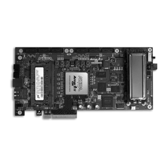
Page 10: Board Overview
2–2 Chapter 2: Board Components Board Overview Board Overview This section provides an overview of the Arria II GX FPGA development board, including an annotated board image and component descriptions. Figure 2–1 provides an overview of the development board features. - Page 11 Chapter 2: Board Components 2–3 Board Overview Table 2–1. Arria II GX FPGA Development Board Components (Part 2 of 3) Board Reference Type Description Illuminates when the MAX II CPLD EPM2210 System Controller is Load LED actively configuring the FPGA.
- Page 12 2–4 Chapter 2: Board Components Board Overview Table 2–1. Arria II GX FPGA Development Board Components (Part 3 of 3) Board Reference Type Description Load image push-button Load image from flash memory to the FGPA based on the switch configuration LED setting.
-
Page 13: Featured Device: Arria Ii Gx Device
Featured Device: Arria II GX Device Featured Device: Arria II GX Device The Arria II GX FPGA development board features the Arria II GX EP2AGX125EF35 device (U19) in a 1152-pin FBGA package. For more information about Arria II device family, refer to the Arria II GX Device Handbook. -
Page 14: Migration Support
Note to Table 2–4: (1) Transceiver signals are not included. Table 2–5 lists the Arria II GX device pin count and usage by function on the development board. Table 2–5. Arria II GX Device Pin Count and Usage Function I/O Standard... -
Page 15: Max Ii Cpld Epm2210 System Controller
Chapter 2: Board Components 2–7 MAX II CPLD EPM2210 System Controller The specific I/O resources available in the Arria II GX EP2AGX260EF35 device are listed in “General User Input/Output” on page 2–24. A second HSMC port is available in the Arria II GX EP2AGX260EF35 device to support an extra transceiver quadrant and additional I/O banks. - Page 16 FSM bus flash memory clock flash_clk FSM bus flash memory output enable flash_oen FSM bus flash memory ready flash_rdy_bsyn FSM bus flash memory reset flash_resetn Arria II GX FPGA Development Board Reference Manual February 2011 Altera Corporation Arrow.com. Arrow.com. Arrow.com. Arrow.com. Arrow.com. Arrow.com.
- Page 17 FSM bus address fsm_a[5] FSM bus address fsm_a[6] FSM bus address fsm_a[7] FSM bus address fsm_a[8] FSM bus address fsm_a[9] February 2011 Altera Corporation Arria II GX FPGA Development Board Reference Manual Arrow.com. Arrow.com. Arrow.com. Arrow.com. Arrow.com. Arrow.com. Arrow.com. Arrow.com. Arrow.com. Arrow.com.
- Page 18 Flash memory image select indicator led_config_led[2] — Toggles the LED_CONFIG_LED[2:0] sequence. factory (IMAGE SEL) — DIP - MAX II LCD drive enable lcd_pwrmon Arria II GX FPGA Development Board Reference Manual February 2011 Altera Corporation Arrow.com. Arrow.com. Arrow.com. Arrow.com. Arrow.com. Arrow.com.
- Page 19 Manufacturer Part Number Website IC - MAX II CPLD EPM2210 Altera Corporation EPM2210F256C3N www.altera.com 256FBGA -3 LF 2.5V VCCINT February 2011 Altera Corporation Arria II GX FPGA Development Board Reference Manual Arrow.com. Arrow.com. Arrow.com. Arrow.com. Arrow.com. Arrow.com. Arrow.com. Arrow.com. Arrow.com.
-
Page 20: Configuration, Status, And Setup Elements
The board implements a USB-Blaster using a USB Type-B connector (J6), a FTDI USB 2.0 PHY device (U15), and an Altera MAX IIZ CPLD (U10). This allows the configuration of the FPGA using a USB cable directly connected between the USB port on the board (J6) and a USB port of a PC running the Quartus II software. - Page 21 GUI interfaces. For this setting, remove the left-most jumper shunt from the JTAG chain header (J9). Flash Memory Programming Flash memory programming is possible through a variety of methods using the Arria II GX device. February 2011 Altera Corporation Arria II GX FPGA Development Board Reference Manual Arrow.com. Arrow.com. Arrow.com. Arrow.com. Arrow.com.
-
Page 22: Fpga Programming From Flash Memory
The PFL megafunction is a block of logic that is programmed into an Altera programmable logic device (FPGA or CPLD). The PFL functions as a utility for writing to a compatible flash memory device. This... - Page 23 Table 2–9. Flash Memory Map (Part 1 of 2) Name Size (KB) Address 0x03FF-FFFF 0x03FF-8000 0x03FF-7FFF 0x03FF-0000 Unused 0x03FE-FFFF 0x03FE-8000 0x03FE-7FFF 0x03FE-0000 February 2011 Altera Corporation Arria II GX FPGA Development Board Reference Manual Arrow.com. Arrow.com. Arrow.com. Arrow.com. Arrow.com. Arrow.com. Arrow.com. Arrow.com. Arrow.com. Arrow.com. Arrow.com. Arrow.com. Arrow.com.
- Page 24 User hardware 1 User hardware 2 Notes to Table 2–10: (1) ON indicates a setting of ’1’. (2) OFF indicates a setting of ’0’. Arria II GX FPGA Development Board Reference Manual February 2011 Altera Corporation Arrow.com. Arrow.com. Arrow.com. Arrow.com. Arrow.com.
-
Page 25: Fpga Programming Over External Usb-Blaster
160 becomes grounded. Driven by the add-in card. PCIe x1 Green LED. Configure this LED to display the PCI Express link width x1. February 2011 Altera Corporation Arria II GX FPGA Development Board Reference Manual Arrow.com. Arrow.com. Arrow.com. -
Page 26: Setup Elements
ON : LCD driven from the MAX II EPM2210 System Controller (power monitor) LCD_PWRMON OFF : LCD driven from the FPGA ON : Embedded USB-Blaster disable USB_DISABLEn OFF : Embedded USB-Blaster enable Arria II GX FPGA Development Board Reference Manual February 2011 Altera Corporation Arrow.com. Arrow.com. Arrow.com. Arrow.com. Arrow.com. -
Page 27: Jtag Chain Header
JTAG Chain Header The JTAG chain header (J9) either remove or include devices in the active JTAG chain by removing or installing the jumper shunts. However, the Arria II GX FPGA device is always in the JTAG chain. Table 2–15 shows the header controls and its descriptions. -
Page 28: Pci Express Control Dip Switch
Description Manufacturer Manufacturer Website Reference Part Number http://www.dawning2.com.tw/ PB4, PB5, PB6 Push-Button switch Dawning Precision Co. TS-A02SA-2-S100 company.php Arria II GX FPGA Development Board Reference Manual February 2011 Altera Corporation Arrow.com. Arrow.com. Arrow.com. Arrow.com. Arrow.com. Arrow.com. Arrow.com. Arrow.com. Arrow.com. Arrow.com. -
Page 29: Clock Circuitry
25 MHz Crystal Crystal Table 2–20 shows the external clock inputs for the Arria II GX FPGA development board. Table 2–20. Arria II GX FPGA Development Board Clock Inputs (Part 1 of 2) Source Schematic Signal Name I/O Standard Description CLK_155_P 155.52 MHz oscillator which drives the... - Page 30 (2) CDCM61004 has a default frequency of 125 MHz, but can also be set by the MAX II CPLD to frequencies of 100 MHz and 156.25 MHz. (3) Transceiver Q3 is only available when the Arria II GX FPGA development board is populated with the EP2AGX260 device.
-
Page 31: Arria Ii Gx Fpga Clock Outputs
EP2AGX125EF35 HSMB_CLKOUT0 (2.5 V) PLL 1 PLL 4 Table 2–21 lists the clock outputs for the Arria II GX FPGA development board. Table 2–21. Arria II GX FPGA Development Board Clock Outputs Connector Schematic Signal Name I/O Standard Description 2.5-V... -
Page 32: General User Input/Output
Board references PB1 and PB2 are push-button switches that allow you to interact with the Arria II GX device. When you press and hold the switch, the device pin is set to logic 0; when you release the switch, the device pin is set to logic 1. There is no board-specific function for these general user push-button switches. -
Page 33: User-Defined Dip Switches
LEDs from the FPGA designs loaded into the Arria II GX device. The LEDs illuminate when a logic 0 is driven, and turns off when a logic 1 is driven. There is no board-specific function for these LEDs. -
Page 34: Hsmc User-Defined Leds
Labeled RX for HSMC port B. Note to Table 2–29: (1) HSMB is only available when the Arria II GX FPGA development board is populated with the EP2AGX260 device. Arria II GX FPGA Development Board Reference Manual February 2011 Altera Corporation Arrow.com. -
Page 35: Lcd
— Power supply GND (0 V) — For LCD drive Register select signal H: Data input L: Instruction input February 2011 Altera Corporation Arria II GX FPGA Development Board Reference Manual Arrow.com. Arrow.com. Arrow.com. Arrow.com. Arrow.com. Arrow.com. Arrow.com. Arrow.com. Arrow.com. -
Page 36: Components And Interfaces
HSMC PCI Express The Arria II GX FPGA development board fits entirely into a PC motherboard with a ×8 PCI Express slot that can accommodate a full height long form factor add-in card. This interface uses the Arria II GX device's PCI Express hard IP block, saving logic resources for the user logic application. - Page 37 The PCIE_REFCLK_P signal is a 100 MHz differential input that is driven from the PC motherboard on to this board through the edge connector. This signal connects directly to a Arria II GX REFCLK input pin pair using DC coupling. This clock is terminated on the motherboard and therefore, no on-board termination is required.
- Page 38 SMB data LVTTL PCIE_SMBDAT — x1 Presence detect PCIE_LED_X1 — x4 Presence detect PCIE_LED_X4 — x8 Presence detect PCIE_LED_X8 Arria II GX FPGA Development Board Reference Manual February 2011 Altera Corporation Arrow.com. Arrow.com. Arrow.com. Arrow.com. Arrow.com. Arrow.com. Arrow.com. Arrow.com. Arrow.com. Arrow.com.
-
Page 39: 10/100/1000 Ethernet
RGMII transmit data ENET_TX_D[1] U24.14 RGMII transmit data ENET_TX_D[2] U24.16 RGMII transmit data ENET_TX_D[3] U24.9 RGMII transmit control ENET_TX_EN February 2011 Altera Corporation Arria II GX FPGA Development Board Reference Manual Arrow.com. Arrow.com. Arrow.com. Arrow.com. Arrow.com. Arrow.com. Arrow.com. Arrow.com. Arrow.com. Arrow.com. Arrow.com. -
Page 40: High-Speed Mezzanine Cards
The development board contains two HSMC interfaces—port A and port B. The HSMC port B is only available if the Arria II GX FPGA development board is populated with the EP2AGX260 device. By default, the board is populated with the EP2AGX125 device and only HSMC port A is available. - Page 41 Dedicated CMOS I/O bit 1 HSMA_D1 J2.43 Dedicated CMOS I/O bit 2 HSMA_D2 J2.44 Dedicated CMOS I/O bit 3 HSMA_D3 February 2011 Altera Corporation Arria II GX FPGA Development Board Reference Manual Arrow.com. Arrow.com. Arrow.com. Arrow.com. Arrow.com. Arrow.com. Arrow.com. Arrow.com.
- Page 42 LVDS or CMOS clock in 1 or CMOS bit 39 HSMA_CLKIN_N1 J2.101 LVDS TX bit 8 or CMOS bit 40 HSMA_TX_D_P8 J2.102 LVDS RX bit 8 or CMOS bit 41 HSMA_RX_D_P8 Arria II GX FPGA Development Board Reference Manual February 2011 Altera Corporation Arrow.com. Arrow.com. Arrow.com. Arrow.com. Arrow.com. Arrow.com.
- Page 43 LVDS or CMOS clock out 2 or CMOS bit 78 HSMA_CLKOUT_N2 J2.158 LVDS or CMOS clock in 2 or CMOS bit 79 HSMA_CLKIN_N2 February 2011 Altera Corporation Arria II GX FPGA Development Board Reference Manual Arrow.com. Arrow.com. Arrow.com. Arrow.com. Arrow.com.
- Page 44 Dedicated CMOS I/O bit 0 AH29 HSMB_D0 J1.42 Dedicated CMOS I/O bit 1 AH30 HSMB_D1 J1.43 Dedicated CMOS I/O bit 2 AK30 HSMB_D2 Arria II GX FPGA Development Board Reference Manual February 2011 Altera Corporation Arrow.com. Arrow.com. Arrow.com. Arrow.com. Arrow.com. Arrow.com. Arrow.com. Arrow.com. Arrow.com.
- Page 45 Dedicated CMOS I/O bit 38 HSMB_D38 J1.98 Dedicated CMOS I/O bit 39 HSMB_D39 J1.101 Dedicated CMOS I/O bit 40 HSMB_D40 February 2011 Altera Corporation Arria II GX FPGA Development Board Reference Manual Arrow.com. Arrow.com. Arrow.com. Arrow.com. Arrow.com. Arrow.com. Arrow.com. Arrow.com.
- Page 46 LVDS or CMOS clock out 2 or CMOS bit 76 HSMB_CLKOUT_P2 J1.156 Dedicated CMOS I/O bit 74 HSMB_D74 J1.157 LVDS or CMOS clock out 2 or CMOS bit 77 HSMB_CLKOUT_N2 Arria II GX FPGA Development Board Reference Manual February 2011 Altera Corporation Arrow.com. Arrow.com. Arrow.com. Arrow.com. Arrow.com. Arrow.com.
-
Page 47: Memory
ASP-122953-01 www.samtec.com family high-speed socket. Memory This section describes the board's memory interface support and also their signal names, types, and connectivity relative to the Arria II GX device. The board has the following memory interfaces: ■ DDR3 ■ DDR2 SODIMM SSRAM ■... - Page 48 DDR3_RST_n U13.L3 Write enable DDR3_WE_n U13.J7 Clock P DDR3_CLK_P Differential 1.5-V SSTL Class I U13.K7 Clock N DDR3_CLK_N Arria II GX FPGA Development Board Reference Manual February 2011 Altera Corporation Arrow.com. Arrow.com. Arrow.com. Arrow.com. Arrow.com. Arrow.com. Arrow.com. Arrow.com. Arrow.com. Arrow.com.
-
Page 49: Ddr2 Sodimm
2 or 4 times the width at full rate or half rate respectively. For example, a 333 MHz 64-bit interface becomes a 166.5 MHz 256-bit bus. February 2011 Altera Corporation Arria II GX FPGA Development Board Reference Manual Arrow.com. Arrow.com. - Page 50 DDR2_CLK_P0 J7.32 Clock N0 DDR2_CLK_N0 Differential 1.8-V SSTL Class I J7.164 Clock P1 DDR2_CLK_P1 J7.166 Clock N1 DDR2_CLK_N1 Arria II GX FPGA Development Board Reference Manual February 2011 Altera Corporation Arrow.com. Arrow.com. Arrow.com. Arrow.com. Arrow.com. Arrow.com. Arrow.com. Arrow.com. Arrow.com. Arrow.com.
- Page 51 AE18 DDR2_DQ26 J7.75 Data bus byte lane 3 AP18 DDR2_DQ27 J7.62 Data bus byte lane 3 AH19 DDR2_DQ28 February 2011 Altera Corporation Arria II GX FPGA Development Board Reference Manual Arrow.com. Arrow.com. Arrow.com. Arrow.com. Arrow.com. Arrow.com. Arrow.com. Arrow.com. Arrow.com. Arrow.com.
- Page 52 AL11 DDR2_DQ55 J7.170 Write mask byte lane 6 AC15 DDR2_DM6 J7.169 Data strobe P byte lane 6 AK13 DDR2_DQS6 Arria II GX FPGA Development Board Reference Manual February 2011 Altera Corporation Arrow.com. Arrow.com. Arrow.com. Arrow.com. Arrow.com. Arrow.com. Arrow.com. Arrow.com. Arrow.com.
-
Page 53: Ssram
Table 2–44 lists the SSRAM pin assignments, signal names, and functions. The signal names and types are relative to the Arria II GX device in terms of I/O setting and direction. Table 2–44. SSRAM Pin Assignments, Schematic Signal Names, and Functions (Part 1 of 3) - Page 54 FSM_D16 U22.D2 Data bus FSM_D17 U22.E1 Data bus FSM_D18 U22.E2 Data bus FSM_D19 U22.F1 Data bus FSM_D20 Arria II GX FPGA Development Board Reference Manual February 2011 Altera Corporation Arrow.com. Arrow.com. Arrow.com. Arrow.com. Arrow.com. Arrow.com. Arrow.com. Arrow.com. Arrow.com. Arrow.com. Arrow.com.
- Page 55 Description Manufacturer Part Number Website Standard synchronous pipelined ISSI Inc. IS61VPS51236A-200B3 www.issi.com SCD, 512K × 36, 200 MHz February 2011 Altera Corporation Arria II GX FPGA Development Board Reference Manual Arrow.com. Arrow.com. Arrow.com. Arrow.com. Arrow.com. Arrow.com. Arrow.com. Arrow.com. Arrow.com. Arrow.com.
-
Page 56: Flash
Table 2–46 lists the flash pin assignments, signal names, and functions. The signal names and types are relative to the Arria II GX device in terms of I/O setting and direction. Table 2–46. Flash Pin Assignments, Schematic Signal Names, and Functions (Part 1 of 2) -
Page 57: Power Supply
An on-board multi-channel analog-to-digital converter (ADC) measures both the voltage and current for several specific board rails. A GUI displays the power utilization by showing a graph of the power consumption versus time. February 2011 Altera Corporation Arria II GX FPGA Development Board Reference Manual Arrow.com. Arrow.com. Arrow.com. -
Page 58: Power Distribution System
3.0 A Maximum 0.143 A 0.091 A A2GX GXB PMA SENSE A2VCCA PLL 2.5 V 0.052 A A2GX Analog PLL BEAD Arria II GX FPGA Development Board Reference Manual February 2011 Altera Corporation Arrow.com. Arrow.com. Arrow.com. Arrow.com. Arrow.com. Arrow.com. Arrow.com. Arrow.com. -
Page 59: Power Measurement
ADC to measure voltage and current. An SPI bus connects these ADC devices to the MAX II CPLD EPM2210 System Controller as well as the Arria II GX FPGA. Figure 2–12 shows the block diagram for the power measurement circuitry. -
Page 60: Statement Of China-Rohs Compliance
(2) X* indicates that the concentration of the hazardous substance of at least one of all homogeneous materials in the parts is above the relevant threshold of the SJ/T11363-2006 standard, but it is exempted by EU RoHS. Arria II GX FPGA Development Board Reference Manual February 2011 Altera Corporation Arrow.com. -
Page 61: Appendix A. Board Revision History
(Speed grade C5NES device) Single-Die Flash Version Differences The single-die flash version of the Arria II GX FPGA development board is created to replace the obsolete dual-die flash device with a single-die flash device. The two flash devices are equivalent except for some software routines used to access them because the single-die device has only one CFI table whereas the duel-die device has two CFI tables. - Page 62 A–2 Appendix A: Board Revision History Single-Die Flash Version Differences Arria II GX FPGA Development Board Reference Manual February 2011 Altera Corporation Arrow.com. Arrow.com. Arrow.com. Arrow.com. Arrow.com. Arrow.com. Arrow.com. Arrow.com. Arrow.com. Arrow.com. Arrow.com. Arrow.com. Arrow.com. Arrow.com. Arrow.com. Arrow.com. Arrow.com. Arrow.com.
-
Page 63: Additional Information
Non-technical support (General) Email nacomp@altera.com (Software Licensing) Email authorization@altera.com Note to Table: (1) You can also contact your local Altera sales office or sales representative. February 2011 Altera Corporation Arria II GX FPGA Development Board Reference Manual Arrow.com. Arrow.com. Arrow.com. Arrow.com. -
Page 64: Typographic Conventions
The envelope links to the Email Subscription Management Center page of the Altera website, where you can sign up to receive update notifications for Altera documents. Arria II GX FPGA Development Board Reference Manual February 2011 Altera Corporation Arrow.com.
Need help?
Do you have a question about the Arria II GX and is the answer not in the manual?
Questions and answers