Renesas RL78/I1D Application Note
Hide thumbs
Also See for RL78/I1D:
- User manual (63 pages) ,
- User manual (3 pages) ,
- User manual (55 pages)
Table of Contents
Advertisement
Quick Links
RL78/I1D
Operation State Switching IAR
Summary
The application note shows the register setting sequence for the switch of RL78/I1D operation state, using the
Operation State Control. After reset, it operates in the LV mode. The flash operation mode is switched one by one by
the button pressing (LV mode → LS mode → HS mode → LS mode → LP mode → LS mode →LV mode, repetition at
the following). The power-supply voltage VDD should be confirmed with the A/D converter when switching to the HS
mode, and if the voltage is out of specified range, the transition should be avoided.
Object device
RL78/I1D
When applying the application note to other microcomputers please change it according to the specification and
evaluate it enough.
R01AN3597EJ0100 Rev.1.00
Jan. 31, 2017
Application note
R01AN3597EJ0100
Rev.1.00
Jan. 31, 2017
Page 1 of 42
Advertisement
Table of Contents

Subscribe to Our Youtube Channel
Related Manuals for Renesas RL78/I1D


Summary of Contents for Renesas RL78/I1D
- Page 1 Jan. 31, 2017 Summary The application note shows the register setting sequence for the switch of RL78/I1D operation state, using the Operation State Control. After reset, it operates in the LV mode. The flash operation mode is switched one by one by the button pressing (LV mode →...
- Page 2 RL78/I1D Operation state switching IAR Contents Specification ............................3 Operation condition confirmation ......................4 Hardware explanation ..........................5 3.1. Example of hardware structure ......................5 3.2. Used pin list ............................. 5 Software explanation ..........................6 4.1. Outline of operation ......................... 6 4.2.
- Page 3 After all the mode RL78/I1D supported operation state transitions are executed, it returns back to the state same as after reset. Table 1.1 shows peripheral function and usage and Figure 1.1 shows the operation state transition sequence order.
- Page 4 ・CPU/peripheral hardware clock: 16MHz, 8MHz, 4MHz, 1 MHz Operation voltage 3.0 V (operable at 1.6V-3.6V). LVD operation (V ): LVD off Integrated development IAR Embedded Workbench for Renesas RL78 V2.21.2 environment C compiler IAR C/C++ Compiler for Renesas RL78 V2.21.1.1833 R01AN3597EJ0100 Rev.1.00 Page 4 of 42...
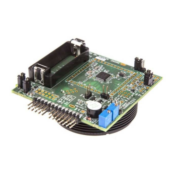
- Page 5 RL78/I1D Operation state switching IAR 3. Hardware explanation 3.1. Example of hardware structure Figure 3.1 shows an example of the hard structure used in the application note RL78/I1D VDD/EVDD RESET LED1 LED2 AVDD INTP0 REGC VSS/EVSS AVSS For on chip debug P40/TOOL0 Figure 3.1...
- Page 6 4.1. Outline of operation In this sample code, the operation state of RL78/I1D is switched by the button pressing (INTP0 interrupt generation). There are 8 kinds of operation states with combination of the flash operation mode and the regulator mode. After 8-time external interrupt INTO0 generations, it returns back to the state same as after reset.
- Page 7 RL78/I1D Operation state switching IAR 4.2. Setting of option byte Table 4.2 shows the setting of option byte. Please set the appropriate value to fit the different system. Table 4.2 Optional byte setting Address Set value Content 000C0H/010C0H 11101111B Watch dog timer operation stop...
- Page 8 RL78/I1D Operation state switching IAR 4.4. List of Variable Table 4.4 lists the global variable that is used by this sample program. Table 4.4 Global variable Type Variable identifier Content Use function uint16_t g_flash_mode State variable of flash operation mode...
-
Page 9: Table Of Contents
RL78/I1D Operation state switching IAR 4.5. Function list Table 4.5 shows the function list. Table 4.5 Function Function name Outline R_MAIN_UserInit The main user initialization R_INTC0_Start INTP0 interrupt enable processing R_IT_Start 12-bit interval timer start processing R_PCLBUZ1_Start Clock output start processing... -
Page 10: The Main User Initialization
RL78/I1D Operation state switching IAR 4.6. Function specification Below shows the function specification of the sample code. R_MAIN_UserInit Outline The main user initialization. Header r_cg_macrodriver.h, r_cg_userdefine.h, r_cg_intc.h, r_cg_it.h, r_cg_pclbuz.h Declaration void R_MAIN_UserInit(void) Explanation Performs initialization necessary to the operation of the application. -
Page 11: A/D Converter Stop Processing
RL78/I1D Operation state switching IAR R_ADC_Stop Outline A/D converter stop processing. Header r_cg_macrodriver.h, r_cg_userdefine.h, r_cg_adc.h Declaration void R_ADC_Stop(void) Explanation Stop the A/D conver operation. Parameter None Return value None switch_flashstatemode_to_LV Outline The flash operation state is switched to the LV mode. -
Page 12: The Flash Operation State Is Switched To The Lp Mode
RL78/I1D Operation state switching IAR switch_flashmode_to_LP Outline The flash operation state is switched to the LP mode. Header r_cg_intc.h Declaration void switch_flashmode_to_LP(void) Explanation The flash operation state is switched to the LP mode. Parameter None Return value None switch_flashstatemode_to_LV_M Outline The flash operation state is switched to the LV mode(MOCO). -
Page 13: 12-Bit Interval Timer Interrupt Processing
RL78/I1D Operation state switching IAR r_it_interrupt Outline 12-bit interval timer interrupt processing Header r_cg_macrodriver.h、r_cg_userdefine.h、r_cg_intc.h、r_cg_intp.h Declaration __interrupt static void r_it_interrupt(void) Explanation LED state is updated according to the state of operation state. Parameter None Return value None R01AN3597EJ0100 Rev.1.00 Page 13 of 42... - Page 14 RL78/I1D Operation state switching IAR 4.7. Flow chart Figure 4.1 shows the whole flowchart. Figure 4.1 Overall Flow 4.7.1. The main processing Figure 4.2 shows the flowchart of main processing. main Initialization setting function hdwinit() Main initialization functionR_MAIN_UserInit() : while(1) loop...
- Page 15 RL78/I1D Operation state switching IAR 4.7.2. Initialization Figure 4.3 shows the flowchart of initialization flow chart. hdwinit Maskable interrupt disable IE ← 0 Port initialization Peripheral function initialization CPU clock initialization R_Systeminit() 12-bit interval timer initialization Clock output initialization External interrupt initialization return Figure 4.3...
- Page 16 RL78/I1D Operation state switching IAR 4.7.3. Peripheral function Initialization Figure 4.4 shows the flowchart of peripheral function initialization. Figure 4.4 Peripheral function initialization 4.7.4. I/O Port Setup Figure 4.5 shows the flowchart of I/O Port Setup. Figure 4.5 I/O Port Setup Caution: Provide proper treatment for unused pins so that their electrical specifications are observed.
- Page 17 Bit 0 PM60 PM60 I/O mode selection Output mode (output buffer on) Input mode (output buffer off) Caution: For details on the register setup procedures, refer to RL78/I1D User's Manual: Hardware. R01AN3597EJ0100 Rev.1.00 Page 17 of 42 Jan. 31, 2017...
- Page 18 RL78/I1D Operation state switching IAR 4.7.5. CPU clock initialization Figure 4.6 shows the flowchart of CPU clock initialization. Figure 4.6 CPU clock initialization Note: Refer to RL78/G13 (R01AN2575J) application note for CPU clock setting (R_CGC_Create()). R01AN3597EJ0100 Rev.1.00 Page 18 of 42...
- Page 19 Crystal resonator connection Input port mode Input port External clock input mode Input port External clock input Caution: For details on the register setup procedures, refer to RL78/I1D User's Manual: Hardware. R01AN3597EJ0100 Rev.1.00 Page 19 of 42 Jan. 31, 2017...
- Page 20 Bit 0 HIOSTOP High-speed on-chip oscillator clock operation control High-speed on-chip oscillator operating High-speed on-chip oscillator stopped Caution: For details on the register setup procedures, refer to RL78/I1D User's Manual: Hardware. R01AN3597EJ0100 Rev.1.00 Page 20 of 42 Jan. 31, 2017...
- Page 21 Caution: The OSMC register is intended to be used to reduce power consumption by reducing the operating current of the device in the STOP and HALT modes while the subsystem clock is selected as CPU clock. For details on the register setup procedures, refer to RL78/I1D User's Manual: Hardware.
- Page 22 MCM1 Main system clock (f ) operation control MAIN High-speed on-chip oscillator clock Middle-speed on-chip oscillator clock Caution: For details on the register setup procedures, refer to RL78/I1D User's Manual: Hardware. R01AN3597EJ0100 Rev.1.00 Page 22 of 42 Jan. 31, 2017...
- Page 23 RL78/I1D Operation state switching IAR 4.7.6. 12-bit interval timer initialization Figure 4.7 shows the flowchart of 12-bit interval timer initialization. R_IT_Create PRR2 register 12-bit interval timer TMKARES bit 1 :12-bit interval timer reset state reset control TMKARES bit 0 :12-bit interval timer reset release...
- Page 24 RL78/I1D Operation state switching IAR 4.7.7. Clock output initialization Figure 4.8 shows the flowchart of clock output initialization. Figure 4.8 clock output initialization 4.7.8. INTP0 initialization Figure 4.9 shows the flowchart of INTP0 initialization. R_INTP0_Create INTPn interrupt disabled PMK6-PMK0 bit...
- Page 25 RL78/I1D Operation state switching IAR 4.7.9. The main user initialization Figure 4.10 shows the flowchart of the main user initialization. Figure 4.10 The main user initialization 4.7.10. INTP0 interrupt enable processing Figure 4.11 shows the flowchart of INTP0 interrupt enable processing.
- Page 26 RL78/I1D Operation state switching IAR 4.7.11. 12-bit interval timer start processing Figure 4.12 shows the flowchart of 12-bit interval timer start processing. Figure 4.12 12-bit interval timer start processing 4.7.12. Clock output start processing Figure 4.13 shows the flowchart of clock output start processing.
- Page 27 RL78/I1D Operation state switching IAR 4.7.13. Flash operation mode switching (LV) processing Figure 4.14 shows the flowchart of the flash operation mode switching (LV) processing. Figure 4.14 Flash operation switching (LV) processing R01AN3597EJ0100 Rev.1.00 Page 27 of 42 Jan. 31, 2017...
- Page 28 FLMWEN Control of regulator mode Rewriting the FLMODE register is disabled Rewriting the FLMODE register is enabled Caution: For details on the register setup procedures, refer to RL78/I1D User's Manual: Hardware. R01AN3597EJ0100 Rev.1.00 Page 28 of 42 Jan. 31, 2017...
- Page 29 RL78/I1D Operation state switching IAR 4.7.14. Flash operation mode switching (LS normal) processing Figure 4.15, Figure 4.16 shows the flowchart of the flash operation mode switching (LS normal). Figure 4.15 Flash operation mode switching (LS normal) processing(1/2) R01AN3597EJ0100 Rev.1.00 Page 29 of 42...
- Page 30 RL78/I1D Operation state switching IAR Figure 4.16 Flash operation mode switching (LS normal) processing(2/2) R01AN3597EJ0100 Rev.1.00 Page 30 of 42 Jan. 31, 2017...
- Page 31 RL78/I1D Operation state switching IAR 4.7.15. Flash operation mode switching (LS low consumption) processing Figure 4.17 shows the flowchart of the flash operation mode switching (LS low consumption) processing. switch_flashmode_to_LS_1 Main on-chip oscillator clock status in the case of MCS1 = 0? high-speed on-chip oscillator clock, switch to the middle-speed on-chip oscillator clock.
- Page 32 RL78/I1D Operation state switching IAR 4.7.16. Flash operation mode switching (HS) processing Figure 4.18, Figure 4.19 shows the flowchart of the flash operation mode switching (HS) processing. switch_flashmode_to_HS PMMC register Set the regulator mode to MCSEL bit the normal setting...
- Page 33 RL78/I1D Operation state switching IAR Second A/D conversion operation start No(branch in g_ad_busy = 1) A/D conversion operation is completed? Maskable interrupt disable A/D converter stop processing R_ADC_Stop() VDD voltage is less than 2.4V ? g_flash_mode Updated status flag variable of...
- Page 34 RL78/I1D Operation state switching IAR 4.7.17. A/D converter initialization Figure 4.20 shows the flowchart of A/D converter initialization. R_ADC_Create PRR0 register Reset control of A/D converter ADCRES bit 1: A/D converter reset state ADCRES bit 0: A/D converter reset release...
- Page 35 RL78/I1D Operation state switching IAR 4.7.18. A/D conversion operation start processing Figure 4.21 shows the flowchart of A/D converter initialization. Figure 4.21 A/D conversion operation start processing 4.7.19. A/D converter stop processing Figure 4.22 shows the flowchart of A/D converter initialization.
- Page 36 RL78/I1D Operation state switching IAR 4.7.20. Flash operation mode switching (LP) processing Figure 4.23 shows the flowchart of the flash operation mode switching (LP) processing. switch_flashmode_to_LP MOCODIV register Set the middle-speed on-chip oscillator clock frequency to 1MHz Main on-chip oscillator clock status in the case of...
- Page 37 RL78/I1D Operation state switching IAR 4.7.21. External interruption (INTP0) processing Figure 4.24, Figure 4.25 shows the flowchart of the external interruption (INTP0) processing. Figure 4.24 External interrupt (INTP0) processing(1/2) R01AN3597EJ0100 Rev.1.00 Page 37 of 42 Jan. 31, 2017...
- Page 38 RL78/I1D Operation state switching IAR Figure 4.25 External interrupt (INTP0) processing(2/2) R01AN3597EJ0100 Rev.1.00 Page 38 of 42 Jan. 31, 2017...
- Page 39 RL78/I1D Operation state switching IAR 4.7.22. 12-bit interval timer interrupt processing Figure 4.26 shows the flowchart of the 12-bit interval timer interrupt processing. r_it_interrupt Variable state g_flash_mode _00_FLASHMODE_LV (LV mode) P6.0(LED0): Turning off P6.1(LED1): Turning on _01_FLASHMODE_LS_0 (LS normal mode) P6.0(LED0): Turning on...
- Page 40 RL78/I1D Operation state switching IAR 4.7.23. A/D conversion complete interrupt processing Figure 4.27 shows the flowchart of the A/D conversion complete interrupt processing. Figure 4.27 A/D conversion complete interrupt processing 4.7.24. A/D conversion result acquisition process Figure 4.28 shows the flowchart of the A/D conversion result acquisition processing.
- Page 41 Power supply current measurement mode can measure the HALT mode. The operation of the power supply current measurement mode RL78/I1D operation state is switched by a button is pressed (INTP0 interrupt generation). Wait for the button press (INTP0 interrupt generation) in HALT mode.
- Page 42 RL78/I1D Operation state switching IAR 6. Sample code Please get the sample code from Renesas Electronics homepage. 7. Reference document RL78/I1D User’s Manual: Hardware (R01UH0474E) RL78 family user's manual software (R01US0015E) (Please get the latest version from Renesas Electronics homepage.) Technical update (Please acquire latest information from Renesas Electronics homepage.)
- Page 43 RL78/I1D Operation state switching IAR modification record Revision Rev. Date Page Summary 1.00 Jan. 31, 2017 — First Edition...
- Page 44 General Precautions in the Handling of Microprocessing Unit and Microcontroller Unit Products The following usage notes are applicable to all Microprocessing unit and Microcontroller unit products from Renesas. For detailed usage notes on the products covered by this document, refer to the relevant sections of the document as well as any technical updates that have been issued for the products.
- Page 45 10. It is the responsibility of the buyer or distributor of Renesas Electronics products, who distributes, disposes of, or otherwise places the product with a third party, to notify such third party in advance of the contents and conditions set forth in this document, Renesas Electronics assumes no responsibility for any losses incurred by you or third parties as a result of unauthorized use of Renesas Electronics products.
Need help?
Do you have a question about the RL78/I1D and is the answer not in the manual?
Questions and answers