Table of Contents
Advertisement
Quick Links
Advertisement
Table of Contents

Subscribe to Our Youtube Channel
Related Manuals for GOWIN DK-START-GW2A55-PG484 V1.3


Summary of Contents for GOWIN DK-START-GW2A55-PG484 V1.3
- Page 1 DK-START-GW2A55-PG484_V1.3 User Guide DBUG375-1.2E, 09/01/2021...
- Page 2 Copyright © 2021 Guangdong Gowin Semiconductor Corporation. All Rights Reserved. , Gowin, and GOWINSEMI are trademarks of Guangdong Gowin Semiconductor Corporation and are registered in China, the U.S. Patent and Trademark Office, and other countries. All other words and logos identified as trademarks or service marks are the property of their respective holders.
- Page 3 Revision History Date Version Description 04/22/2020 1.0E Initial version published. The name of the board updated; 01/06/2020 1.1E The description of chapter 3.1 FPGA Module updated. 09/01/2021 1.2E The quick start in 2.2 Development Board Suite removed.
-
Page 4: Table Of Contents
Contents Contents Contents ....................... i List of Figures ....................iv List of Tables ...................... vi 1 About This Guide ..................... 1 1.1 Purpose ..........................1 1.2 Related Documents ......................1 1.3 Terminology and Abbreviations ................... 1 1.4 Support and Feedback ....................... 2 2 Introduction ...................... - Page 5 Contents 3.5.1 Introduction ........................12 3.5.2 Pinout ..........................12 3.6 Ethernet ..........................14 3.6.1 Introduction ........................14 3.6.2 Pinout ..........................14 3.7 LVDS Interfaces ........................ 15 3.7.1 Introduction ........................15 3.7.2 Pinout ..........................16 3.8 MIPI DSI ........................... 17 3.8.1 Introduction ........................17 3.8.2 Pinout ..........................
- Page 6 Contents 3.16 Industry Screen Interface ....................27 3.16.1 Introduction ........................27 3.16.2 Pinout ........................... 28 3.17 LED Module ........................29 3.17.1 Introduction ........................29 3.17.2 Pinout ........................... 29 3.18 Keys Module ........................29 3.18.1 Introduction ........................29 3.18.2 Pinout ........................... 30 3.19 Switches Module ......................
-
Page 7: List Of Figures
List of Figures List of Figures Figure 2-1 DK-START-GW2A55-PG484_V1.3 Development Board ..........3 Figure 2-2 Development Kit ....................... 4 Figure 2-3 PCB Components ......................5 Figure 2-4 System Block Diagram ..................... 5 Figure 3-1 Connection Diagram of FPGA Downloading and Configuration ........9 Figure 3-2 Asynchronous FIFO Connection Diagram ................ - Page 8 List of Figures Figure 4-2 Process Window ....................... 33 Figure 4-3 Build Completed ....................... 33 Figure 4-4 Programmer Window ......................34 Figure 4-5 Device Configure Window ....................34 Figure 4-6 Click Program/Configure ....................34 DBUG375-1.2E...
- Page 9 List of Tables List of Tables Table 1-1 Abbreviations and Terminology ..................2 Table 3-1 FPGA Download and Pinout ....................9 Table 3-2 Asynchronous FIFO Pinout ....................10 Table 3-3 Clock and Reset Pinout...................... 11 Table 3-4 DDR3 Pinout ........................12 Table 3-5 Ethernet Pinout ........................
-
Page 10: About This Guide
UG113, GW2A-55 Pinout UG111, GW2A series of FPGA Products Package and Pinout User Guide UG290, Gowin FPGA Products Programming and Configuration Guide SUG100, Gowin Software User Guide 1.3 Terminology and Abbreviations The terminology and abbreviations used in this manual are as shown in Table 1-1. -
Page 11: Support And Feedback
Low-Voltage Differential Signaling SSRAM Shadow Static Random Access Memory 1.4 Support and Feedback Gowin Semiconductor provides customers with comprehensive technical support. If you have any questions, comments, or suggestions, please feel free to contact us directly by the following ways. Website: www.gowinsemi.com... -
Page 12: Introduction
The development board uses the GW2A- LV55PG484 FPGA device, which is the first generation product of Gowin Arora family. The GW2A series of FPGA products offer a range of features and rich resources like high-performance DSP, high-speed LVDS interface and BSRAM. -
Page 13: Development Board Suite
2 Introduction 2.2 Development Board Suite GW2A- LV55PG484 development board includes a DDR3 chip with 2Gbit, 16-bit bus width. Its two Gigabit Ethernet interfaces support 10M, 100M, 1000M Ethernet communication. It has abundant peripheral interfaces, including LVDS interfaces, a SD card socket, CAN bus interface, MIPI CSI, MIPI DSI, AD/DA interface and GPIO interfaces. -
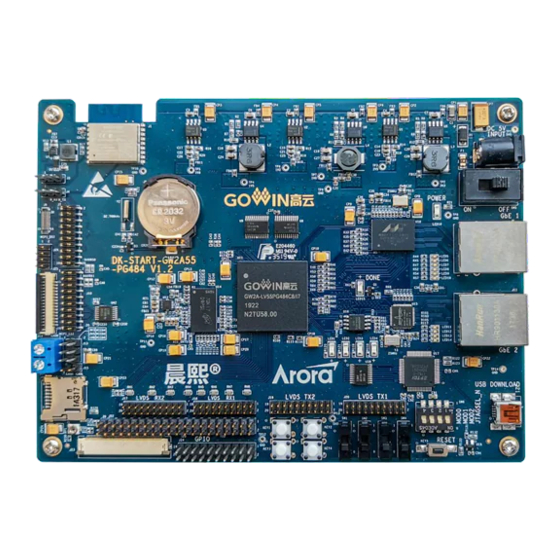
Page 14: Pcb Components
2 Introduction 2.3 PCB Components 2.3 PCB Components Figure 2-3 PCB Components 1.8V Power 1.2V Power 2.5V Power Button Cell 1.5V Power 1.0V Power 3.3V Power Power WIFI Socket Power Switch Ethernet 1 AD/DA DDR3 Ethernet 2 Bank4 Level LED*4 Select CAN Interface USB MINI B... -
Page 15: Features
2 Introduction 2.5 Features 2.5 Features The key features are as follows: 1. The FPGA device Gowin GW2A-LV55PG484 FPGA Max. user I/O 319 2. Download and Boot Integrates the download module and can be downloaded with USB ... - Page 16 2 Introduction 2.5 Features double row of pins with 2.00mm pitch. 9. MIPI CSI Interface MIPI interface includes 3 pairs of differential signals, among which one for clock and four for data. 15pin FPC connector with 1mm pitch is used. ...
-
Page 17: Development Board Circuit
3 Development Board Circuit 3.1 FPGA Module Development Board Circuit 3.1 FPGA Module Overview For the resources of GW2A-LV55PG484 FPGA products, see DS102, GW2A series FPGA Products Data Sheet. I/O BANK Introduction For the I/O BANK, package and pinout information, see UG111, GW2A series of FPGA Products Package and Pinout User Guide. -
Page 18: Pinout
3 Development Board Circuit 3.2 Download Module Figure 3-1 Connection Diagram of FPGA Downloading and Configuration By configuring EEPROM chip, the B channel of FT2232 can be configured as an asynchronous FIFO interface. The connection diagram is follows. Figure 3-2 Asynchronous FIFO Connection Diagram FTDI_SIWU# USB_D+ FTDI_WR#... -
Page 19: Power Supply
3 Development Board Circuit 3.3 Power Supply Name FPGA Pin No. BANK I/O Level Description Configure FLASH_SPI_CS_N 1.5V FLASH Signal Configure FLASH_SPI_CLK 1.5V FLASH Signal Table 3-2 Asynchronous FIFO Pinout Name FPGA Pin No. BANK I/O Level Description Send/wake up FTDI_SIWU# 1.2V signal... -
Page 20: Clock And Reset
3 Development Board Circuit 3.4 Clock and Reset 1.8v and 1.2v, and the maximum output current is 2A. One TPS51200 power chip is used to generate 0.75v power for DDR3 chip. One APW7136CCI power chip is used to generate 9.9v power for RGB industry screen. -
Page 21: Ddr3
3 Development Board Circuit 3.5 DDR3 3.5 DDR3 3.5.1 Introduction The development board includes a DDR3 chip with 2Gbit, 16-bit bus width, and the highest data rate is 1600MT/s. Figure 3-4 Connection Diagram of FPGA and DDR3 3.5.2 Pinout Table 3-4 DDR3 Pinout Name FPGA Pin No. - Page 22 3 Development Board Circuit 3.5 DDR3 Name FPGA Pin No. BANK I/O Level Description Bank address DDR3_BA0 1.5V Bank address DDR3_BA1 1.5V Bank address DDR3_BA2 1.5V DDR3_CASn 1.5V Column address strobe Clock Enable DDR3_CK_EN 1.5V Differential clock DDR3_CKn 1.5V Differential clock DDR3_CKp 1.5V Data...
-
Page 23: Ethernet
3 Development Board Circuit 3.6 Ethernet 3.6 Ethernet 3.6.1 Introduction The development board has two Ethernet circuits and supports gigabit mode, which can provide hardware testing environment in the LED display applications. The interface connected to other devices is RJ45 and the transformer is integrated. -
Page 24: Lvds Interfaces
3 Development Board Circuit 3.7 LVDS Interfaces Name FPGA BANK Description Pin No. Level PHY1_RXD2 3.3V PHY1 receiving data channel 2 PHY1_RXD3 3.3V PHY1 receiving data channel 3 PHY1_RX_DV 3.3V PHY1 receiving data enable PHY2_GTCLK 3.3V PHY2 transmitting clock PHY2_TXD0 3.3V PHY2 transmitting data channel 0 PHY2_TXD1... -
Page 25: Pinout
3 Development Board Circuit 3.7 LVDS Interfaces Figure 3-7 LVDS RX Interface 3.7.2 Pinout Table 3-6 LVDS TX Pinout Name FPGA BANK I/O Level Description Pin No. LVDS_B1_P 2.5V Differential Channel 1+ LVDS_B1_N 2.5V Differential Channel 1- LVDS_B2_P 2.5V Differential Channel 2+ LVDS_B2_N 2.5V Differential Channel 2-... -
Page 26: Mipi Dsi
3 Development Board Circuit 3.8 MIPI DSI Table 3-8 LVDS TX2 Pinout Name FPGA BANK I/O Level Description Pin No. 2.5V Differential Channel 1+ LVDS_A1_P 2.5V Differential Channel 1- LVDS_A1_N 2.5V Differential Channel 2+ LVDS_A2_P 2.5V Differential Channel 2- LVDS_A2_N 2.5V Differential Channel 3+ LVDS_A3_P... -
Page 27: Pinout
3 Development Board Circuit 3.8 MIPI DSI Figure 3-8 Connection Diagram of MIPI DSI DSI_LP_D0n DSI_D0n DSI_LP_D0p DSI_D0p DSI_D0n DSI_D0p DSI_LP_D1n DSI_D1n DSI_LP_D1p DSI_D1p DSI_D1n DSI_D1p DSI_LP_D2n DSI_D2n DSI_CLKn DSI_CLKp DSI_LP_D2p DSI_D2p DSI_D2n DSI_RSTn DSI_LP_D3n DSI_D3n DSI_D2p DSI_CABC DSI_LP_D3p DSI_D3p DSI_TE DSI_D3n DSI_D3p... -
Page 28: Mipi Csi
3 Development Board Circuit 3.9 MIPI CSI Name FPGA Pin No. BANK I/O Level Description DSI_LP_D1n 1.2V LP single-ended data 1 DSI_LP_D1p 1.2V LP single-ended data 1 DSI_LP_CLKn B6 1.2V LP single-ended clock DSI_LP_CLKp D7 1.2V LP single-ended clock DSI_LP_D2n 1.2V LP single-ended data 2 DSI_LP_D2p... -
Page 29: Pinout
3 Development Board Circuit 3.10 SD Card 3.9.2 Pinout Table 3-11 MIPI DSI Pinout Name FPGA Pin No. BANK I/O Level Description CSI_D0n 2.5V HS differential data 0- CSI_D0p 2.5V HS differential data 0+ CSI_D1n 2.5V HS differential data 1 CSI_D1p 2.5V HS differential data 1+... -
Page 30: Pinout
3 Development Board Circuit 3.11 RTC 3.10.2 Pinout Table 3-12 SD Card Pinout Name FPGA Pin No. BANK I/O Level Description SD_D0 3.3V Data bit 0 SD_D1 3.3V Data bit 1 SD_D2 3.3V Data bit 2 SD_CD/D3 3.3V Card detection/Data bit 3 SD_CMD 3.3V Commands/Response... -
Page 31: Ad/Da
3 Development Board Circuit 3.12 AD/DA 3.12 AD/DA 3.12.1 Introduction The AD/DA module uses a chip that is a 12-bit A/D and D/A converter with configurable 8-channel interface, which can be configured as any combination of ADC/DAC/GPIO and shares the I2C bus with the RTC module. -
Page 32: Pinout
3 Development Board Circuit 3.14 WIFI Figure 3-13 Connection Diagram of CAN 3.13.2 Pinout Table 3-15 CAN Pinout Name FPGA Pin No. BANK I/O Level Description CAN_TXD 2.5V Transmitting data CAN_RXD 2.5V Receiving data 3.14 WIFI 3.14.1 Introduction The WIFI module supports SPI and UART. SPI transmission rate is 20Mbps. -
Page 33: Gpio
3 Development Board Circuit 3.15 GPIO Name FPGA Pin No. BANK I/O Level Description WIFI_TX 1.2V UART transmitting WIFI_RX 1.2V UART receiving 3.15 GPIO 3.15.1 Introduction 34 GPIOs channeled by two double-column pins with 2.54mm pitch are reserved on the development board for testing. The 40pin interfaces are connected to Bank5. -
Page 34: Pinout
3 Development Board Circuit 3.15 GPIO Figure 3-16 20pin Diagram 3.15.2 Pinout Table 3-17 40pin Interface Pinout Pin No. Name FPGA Pin No. BANK I/O Level Description 3.3V General I/O H_GPIO_01 AA11 3.3V General I/O H_GPIO_02 3.3V General I/O H_GPIO_03 AB11 3.3V General I/O... -
Page 35: Table 3-18 20Pin Interface Pinout
3 Development Board Circuit 3.15 GPIO Pin No. Name FPGA Pin No. BANK I/O Level Description 3.3V General I/O H_GPIO_22 3.3V General I/O H_GPIO_23 3.3V General I/O H_GPIO_24 3.3V General I/O H_GPIO_25 3.3V General I/O H_GPIO_26 3.3V General I/O H_GPIO_27 3.3V General I/O H_GPIO_28... -
Page 36: Industry Screen Interface
3 Development Board Circuit 3.16 Industry Screen Interface 3.16 Industry Screen Interface 3.16.1 Introduction This interface uses 50pin FPC connector with 0.5mm pitch. The pin definition conforms to the industry screen of AT070TN92 model, and all I/O and 40PIN multiplex GPIO of FPGA. Figure 3-17 50pin FPC Interface Diagram LED+ LED+... -
Page 37: Pinout
3 Development Board Circuit 3.16 Industry Screen Interface 3.16.2 Pinout Table 3-19 50pin FPC Interface Pinout Name FPGA BANK Description Pin No. Level LCD_MODE 3.3V DE or SYNC mode selection LCD_DE 3.3V Data input enable LCD_VS 3.3V Column synchronization signal LCD_HS 3.3V Row synchronization signal... -
Page 38: Led Module
3 Development Board Circuit 3.17 LED Module 3.17 LED Module 3.17.1 Introduction There are four blue LED lights on the development board, which can be used for demo. When the output signal of FPGA corresponding pin is low, the LED is lit up. When the output signal is high, the LED is off. The connection diagram is shown in Figure 3-18. -
Page 39: Pinout
3 Development Board Circuit 3.19 Switches Module Figure 3-19 Key Circuit Diagram 3.18.2 Pinout Table 3-22 Keys Module Pinout Name FPGA Pin No. BANK I/O Level Description KEY1 1.5V KEY1 KEY2 1.5V KEY2 KEY3 1.5V KEY3 KEY4 1.5V KEY4 3.19 Switches Module 3.19.1 Introduction There are four switches on the development board to control input during testing. -
Page 40: Pinout
3 Development Board Circuit 3.19 Switches Module 3.19.2 Pinout Table 3-23 Switches Module Pinout Name FPGA Pin No. BANK I/O Level Description 1.5V Switch1 1.5V Switch2 AB21 1.5V Switch3 1.5V Switch4 DBUG375-1.2E 31(34) -
Page 41: Quick Start
4 Quick Start 4.1 Install Software Quick Start 4.1 Install Software Install Gowin EDA software (Gowin Software) to create, build and download FPGA Demo program. Download the EDA software, apply for a license, and obtain software user guide at GOWINSEMI website https://www.gowinsemi.com/en/support/home/. -
Page 42: Figure 4-1 Design Window
4 Quick Start 4.3 Build Demo Program Figure 4-1 Design Window 2. Right click "Place & Route" in the "Process" window and select "Rerun All". Figure 4-2 Process Window 3. After building, the following information will be displayed. The generated bitstream file is saved in: ..LED_test\impl\pnr\LED_test.fs. Figure 4-3 Build Completed DBUG375-1.2E 33(34) -
Page 43: Download And Run
4 Quick Start 4.4 Download and Run 4.4 Download and Run 1. Connect the development board with PC using the download cable and switch on the power. Double click "Program Device" in the "Process" window, and the "Programmer" window will pop up. Right click the device list, and select "Configure Device".
Need help?
Do you have a question about the DK-START-GW2A55-PG484 V1.3 and is the answer not in the manual?
Questions and answers