
Subscribe to Our Youtube Channel
Related Manuals for GOWIN DK START GW5ASTLV138FPG676A V1.0


Summary of Contents for GOWIN DK START GW5ASTLV138FPG676A V1.0
- Page 1 DK_START_GW5AST- LV138FPG676A_V1.0 Daughter Board User guide DBUG1272-1.0E, 7/22/2024...
- Page 2 Copyright © 2024 Guangdong Gowin Semiconductor Corporation. All Rights Reserved. is the trademark of Guangdong Gowin Semiconductor Corporation and are registered in China, the U.S. Patent and Trademark Office, and other countries. All other words and logos identified as trademarks or service marks are the property of their respective holders.
- Page 3 Revision History Date Version Description 7/22/2024 1.0E Initial version published.
-
Page 4: Table Of Contents
Contents Contents Contents ....................... i List of Figures ....................iv List of Tables ...................... vi 1 About This Guide ..................... 1 1.1 Purpose ..........................1 1.2 Related Documents ......................1 1.3 Terminology and Abbreviations ................... 2 1.4 Support and Feedback ....................... 2 2 IES Daughter Board .................. - Page 5 Contents 3.1.3 PCB Components ......................27 3.1.4 System Block Diagram ....................28 3.1.5 Features ......................... 28 3.2 Daughter Board Circuit ..................... 29 3.2.1 Power Supply ......................... 29 3.2.2 Clock ..........................30 3.2.3 HDMI Interface ....................... 30 3.2.4 SDI Interface ........................32 3.2.5 Ethernet .........................
- Page 6 Contents 5.2.3 GPIO ..........................65 5.2.4 Board-to-board connector ....................67 6 EDP Daughter Board ..................82 6.1 Introduction ........................82 6.1.1 Overview ........................82 6.1.2 A Daughter Board Kit ..................... 83 6.1.3 PCB Components ......................83 6.1.4 System Block Diagram ....................84 6.1.5 Features .........................
-
Page 7: List Of Figures
List of Figures List of Figures Figure 2-1 EVAL_GW5AT-LV138KFPG676ES_Dcard_IES_V1.0 Daughter Board ......3 Figure 2-2 A Daughter Board Kit ......................4 Figure 2-3 PCB Components ......................4 Figure 2-4 System Block Diagram ..................... 5 Figure 2-5 Power Supply System Distribution ................... 6 Figure 2-6 Clock Connection Diagram .................... - Page 8 List of Figures Figure 4-5 Connection Diagram of MIPI CSI Interface ..............54 Figure 5-1 EVAL_GW5AT-LV138KFPG676ES_Dcard_DVI_SLVS_V1.0 Daughter Board ....60 Figure 5-2 A Daughter Board Kit ......................61 Figure 5-3 PCB Components ......................61 Figure 5-4 System Block Diagram ..................... 62 Figure 5-5 Power Supply System Distribution Diagram..............
- Page 9 List of Tables List of Tables Table 1-1 Terminology and Abbreviations ..................2 Table 2-1 Clock Pin Distribution ......................7 Table 2-2 Ethernet Interface J13 Pin Distribution ................8 Table 2-3 Ethernet Interface J14 Pin Distribution ................8 Table 2-4 Ethernet Interface J15 Pin Distribution ................9 Table 2-5 ELVDS Interface Pin Distribution ..................
- Page 10 List of Tables Table 6-3 J1 Pin Distribution for HDMI-TX Interface ................89 Table 6-4 J5 Pin Distribution for GPIO Connector ................90 Table 6-5 Pin Distribution for RE1 Board-to-Board Connector ............91 DBUG1272-1.0E...
-
Page 11: About This Guide
1 About This Guide 1.1 Purpose About This Guide 1.1 Purpose The DK_START_GW5AST-LV138FPG676A_V1.0 Daughter Board User Guide describes the five daughter boards for the DK_START_GW5AST-LV138FPG676A_V1.0: 1. EVAL_GW5AT-LV138KFPG676ES_Dcard_IES_V1.0 (hereinafter referred to as IES daughter board) 2. EVAL_GW5AT-LV138KFPG676ES_Dcard_SDI_SGMII_V1.0 (hereinafter referred to as SDI daughter board) 3. -
Page 12: Terminology And Abbreviations
Gowin Programmable Input/Output LVDS Low-Voltage Differential Signaling 1.4 Support and Feedback Gowin Semiconductor provides customers with comprehensive technical support. If you have any questions, comments, or suggestions, please feel free to contact us directly using the information provided below. Website: www.gowinsemi.com... -
Page 13: Ies Daughter Board
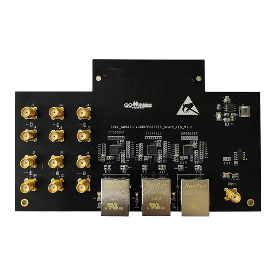
2 IES Daughter Board 2.1 Introduction IES Daughter Board 2.1 Introduction 2.1.1 Overview Figure 2-1 EVAL_GW5AT-LV138KFPG676ES_Dcard_IES_V1.0 Daughter Board The IES daughter board needs to be used with the DK_START_GW5AST-LV138FPG676A_V1.0 motherboard, primarily for Ethernet communication, LVDS communication, and IES evaluation. DBUG1272-1.0E 3(104) -
Page 14: A Daughter Board Kit
2 IES Daughter Board 2.1 Introduction 2.1.2 A Daughter Board Kit The daughter board kit includes the following item: EVAL_GW5AT-LV138KFPG676ES_Dcard_IES_V1.0 daughter board Figure 2-2 A Daughter Board Kit ① EVAL_GW5AT- LV138KFPG676ES_Dcard_IES_V1.0 daughter board 2.1.3 PCB Components Figure 2-3 PCB Components FMC Connector Board Back 1.2V... -
Page 15: System Block Diagram
2 IES Daughter Board 2.1 Introduction 2.1.4 System Block Diagram Figure 2-4 System Block Diagram 2.1.5 Features The key features are as follows: 1. Power The motherboard provides DC 3.3V power The green Power light is on after power on 2. -
Page 16: Daughter Board Circuit
2 IES Daughter Board 2.2 Daughter Board Circuit 2.2 Daughter Board Circuit 2.2.1 Power Supply 2.2.1.1 Introduction The motherboard supplies 3.3V power to the daughter board through the FMC connector. The input 3.3V power generates a 1.2V power supply through the power chip on the IES daughter board to meet the power requirements of the IES daughter board. -
Page 17: Ethernet
2 IES Daughter Board 2.2 Daughter Board Circuit Figure 2-6 Clock Connection Diagram 2.2.2.2 Pin Distribution Table 2-1 Clock Pin Distribution Device Number Signal Name Description 25MHz 25MHz single-ended clock 2.2.3 Ethernet 2.2.3.1 Introduction The IES daughter board provides three Ethernet interfaces, supporting 10BASE-T/100BASE-TX modes. -
Page 18: Table 2-2 Ethernet Interface J13 Pin Distribution
2 IES Daughter Board 2.2 Daughter Board Circuit 2.2.3.2 Pin Distribution Table 2-2 Ethernet Interface J13 Pin Distribution FPGA Signal Name BANK Description Pin No. Level Pin No. Transmit data Transmit data Receive data Receive data Floating VCC3P3 3.3V Power Connection/active F_PHY2_LINKACT0 3.3V... -
Page 19: Elvds Interface
2 IES Daughter Board 2.2 Daughter Board Circuit FPGA Signal Name BANK Description Pin No. Level Pin No. Floating Table 2-4 Ethernet Interface J15 Pin Distribution FPGA Signal Name BANK Description Pin No. Level Pin No. Transmit data Transmit data Receive data Receive data Floating... -
Page 20: Figure 2-8 Connection Diagram Of Elvds Interface
2 IES Daughter Board 2.2 Daughter Board Circuit Figure 2-8 Connection Diagram of ELVDS Interface ELV DS_D0n ELV DS_D3n ELV DS_D0p ELV DS_D3p ELV DS_D1n ELV DS_D4n Connector ELV DS_D1p ELV DS_D4p ELV DS_D2n ELV DS_D5n ELV DS_D2p ELV DS_D5p 2.2.4.2 Pin Distribution Table 2-5 ELVDS Interface Pin Distribution FPGA... -
Page 21: Board-To-Board Connector
2 IES Daughter Board 2.2 Daughter Board Circuit 2.2.5 Board-to-board connector 2.2.5.1 Introduction The IES daughter board has a 400Pin FMC board-to-board connector with 1.27mm pitch for communication with the DK_START_GW5AST- LV138FPG676A_V1.0 motherboard. 2.2.5.2 Pin Distribution Table 2-6 Pin Distribution for RE1 Board-to-Board Connector FPGA Signal Name BANK... - Page 22 2 IES Daughter Board 2.2 Daughter Board Circuit FPGA Signal Name BANK Description Pin No. Level Pin No. Floating Floating Floating Floating Floating Floating Floating Floating Floating Floating Floating Floating Floating Floating Floating DBUG1272-1.0E 12(104)
- Page 23 2 IES Daughter Board 2.2 Daughter Board Circuit FPGA Signal Name BANK Description Pin No. Level Pin No. Floating Floating Floating Floating Floating Floating Floating Floating Floating Floating Floating Floating Floating Floating Floating DBUG1272-1.0E 13(104)
- Page 24 2 IES Daughter Board 2.2 Daughter Board Circuit FPGA Signal Name BANK Description Pin No. Level Pin No. Floating Floating ELVDS differential ELVDS_D0p 3.3V signal 0+ ELVDS differential ELVDS_D0n 3.3V signal 0- Floating Floating Floating Floating F_PHY_MDC 3.3V MII clock input MII data F_PHY_MDIO 3.3V...
- Page 25 2 IES Daughter Board 2.2 Daughter Board Circuit FPGA Signal Name BANK Description Pin No. Level Pin No. Floating Floating VCC3P3 Power Floating Floating Floating ELVDS differential ELVDS_D4p 3.3V signal 4+ ELVDS differential ELVDS_D4n 3.3V signal 4- ELVDS differential ELVDS_D2p 3.3V signal 2+ ELVDS differential...
- Page 26 2 IES Daughter Board 2.2 Daughter Board Circuit FPGA Signal Name BANK Description Pin No. Level Pin No. Floating Floating Floating Floating Floating F_PHY3_RXER 3.3V MII receiving error Floating Floating Floating Floating Floating Floating Floating VCC3P3 Power VCC3P3 Power VCC3P3 Power Floating Floating...
- Page 27 2 IES Daughter Board 2.2 Daughter Board Circuit FPGA Signal Name BANK Description Pin No. Level Pin No. F_PHY1_TXD2 3.3V MII transmit data F_PHY1_TXD1 3.3V MII transmit data F_PHY1_TXD0 AA22 3.3V MII transmit data MII transmit F_PHY1_TXEN AA23 3.3V enable F_PHY1_RXC 3.3V MII receive clock...
- Page 28 2 IES Daughter Board 2.2 Daughter Board Circuit FPGA Signal Name BANK Description Pin No. Level Pin No. Floating Floating External clock F_PHY1_CLK 3.3V input Connection status F_PHY1_Link 3.3V indicator MII collision F_PHY1_COL 3.3V detection F_PHY1_TXD3 3.3V MII transmit data Floating F_PHY1_RXD3 3.3V...
- Page 29 2 IES Daughter Board 2.2 Daughter Board Circuit FPGA Signal Name BANK Description Pin No. Level Pin No. Floating Floating Floating Floating Floating Floating Floating Floating Floating Floating Floating Floating Floating ELVDS differential ELVDS_D5p 3.3V signal 5+ ELVDS differential ELVDS_D5n 3.3V signal 5- ELVDS differential...
- Page 30 2 IES Daughter Board 2.2 Daughter Board Circuit FPGA Signal Name BANK Description Pin No. Level Pin No. Floating Floating Floating Floating Floating Floating F_PHY3_RST_n 3.3V On-chip reset F_PHY3_TXD3 3.3V MII transmit data F_PHY3_TXD2 3.3V MII transmit data F_PHY3_TXD0 3.3V MII transmit data F_PHY3_TXC 3.3V...
- Page 31 2 IES Daughter Board 2.2 Daughter Board Circuit FPGA Signal Name BANK Description Pin No. Level Pin No. Floating Floating Floating Floating ELVDS differential ELVDS_D3p 3.3V signal 3+ ELVDS differential ELVDS_D3n 3.3V signal 3- Floating Floating Floating Floating Floating Floating Floating Floating F_PHY3_CRS...
- Page 32 2 IES Daughter Board 2.2 Daughter Board Circuit FPGA Signal Name BANK Description Pin No. Level Pin No. Floating MII receive data, F_PHY3_RXDV 3.3V valid F_PHY3_RXD1 3.3V MII receive data Connection status F_PHY3_Link 3.3V indicator F_A0 3.3V Chip address A0 F_A1 3.3V Chip address A1...
- Page 33 2 IES Daughter Board 2.2 Daughter Board Circuit FPGA Signal Name BANK Description Pin No. Level Pin No. F_PHY2_TXC AB25 3.3V MII transmit clock F_PHY2_RXC 3.3V MII receive clock MII receive data, F_PHY2_RXDV 3.3V valid F_PHY2_RXD2 3.3V MII receive data F_PHY2_LINKA Connection/active 3.3V...
- Page 34 2 IES Daughter Board 2.2 Daughter Board Circuit FPGA Signal Name BANK Description Pin No. Level Pin No. Floating Floating Connection status F_PHY2_Link 3.3V indicator MII collision F_PHY2_COL 3.3V detection Floating Floating F_PHY2_TXD0 3.3V MII transmit data External clock F_PHY2_CLK 3.3V input External clock...
- Page 35 2 IES Daughter Board 2.2 Daughter Board Circuit FPGA Signal Name BANK Description Pin No. Level Pin No. Floating Floating Floating Floating Floating Floating DBUG1272-1.0E 25(104)
-
Page 36: Sdi Daughter Board
3 SDI Daughter Board 3.1 Introduction SDI Daughter Board 3.1 Introduction 3.1.1 Overview Figure 3-1 EVAL_GW5AT-LV138KFPG676ES_Dcard_SDI_SGMII_V2.1 Daughter Board The SDI daughter board needs to be used with the DK_START_GW5AST-LV138FPG676A_V1.0 motherboard, primarily for HDMI communication, SDI communication, and SGMII communication. The SDI daughter board supports 3Gbps SDI data transfer. DBUG1272-1.0E 26(104) -
Page 37: A Daughter Board Kit
3 SDI Daughter Board 3.1 Introduction 3.1.2 A Daughter Board Kit The daughter board kit includes the following item: EVAL_GW5AT-LV138KFPG676ES_Dcard_SDI_SGMII_V2.1 daughter board Figure 3-2 A Daughter Board Kit ① EVAL_GW5AT- LV138KFPG676ES_Dcard_SDI_SGMII_V2.1 daughter board 3.1.3 PCB Components Figure 3-3 PCB Components 2.5V SDI-OUT SGMII-OUT SGMII-IN 1.0V... -
Page 38: System Block Diagram
3 SDI Daughter Board 3.1 Introduction 3.1.4 System Block Diagram Figure 3-4 System Block Diagram 3.1.5 Features The key features are as follows: 1. Power External DC 5V Power The green Power light is on after power on 2. -
Page 39: Daughter Board Circuit
3 SDI Daughter Board 3.2 Daughter Board Circuit 3.2 Daughter Board Circuit 3.2.1 Power Supply 3.2.1.1 Introduction The SDI daughter board is powered by an external 5V power adapter. The input 5V power generates a 3.3V, 2.5V, 1.8V, 1.0V power supply through the power chip on the SDI daughter board to meet the power requirements of the SDI daughter board. -
Page 40: Clock
3 SDI Daughter Board 3.2 Daughter Board Circuit 3.2.2 Clock 3.2.2.1 Introduction The SDI daughter board provides one 148.5MHz differential clock. The clock signal is let out through two SMA females. Figure 3-6 Clock Connection Diagram 3.2.2.2 Pin Distribution Table 3-1 Clock Pin Distribution Device Signal Name Description... -
Page 41: Table 3-2 J2 Pin Distribution For Hdmi-Tx Interface
3 SDI Daughter Board 3.2 Daughter Board Circuit 3.2.3.2 Pin Distribution Table 3-2 J2 Pin Distribution for HDMI-TX Interface J2 Pin No. Signal Name I/O Level Description HDMI_TXA2P 3.3V HDMI differential data HDMI_TXA2N 3.3V HDMI differential data HDMI_TXA1P 3.3V HDMI differential data HDMI_TXA1N 3.3V HDMI differential data... -
Page 42: Sdi Interface
3 SDI Daughter Board 3.2 Daughter Board Circuit 3.2.4 SDI Interface 3.2.4.1 Introduction The SDI daughter board provides one SDI input interface and one SDI output interface. The SDI-IN interface receives serial data from one BNC female and sends the processed serial data via two SMA females; the SDI-OUT interface receives serial data from two SMA females and sends the processed serial data via one BNC female. -
Page 43: Ethernet
3 SDI Daughter Board 3.2 Daughter Board Circuit Table 3-4 SDI-OUT Interface Pin Distribution Device Number Signal Name I/O Level Description 1218_SDI+ 2.5V SDI+ 1218_SDI- 2.5V SDI- 1218_SDO+ 2.5V SDO+ 3.2.5 Ethernet 3.2.5.1 Introduction The SDI daughter board provides two Ethernet interfaces, supporting 10BASE-T/100BASE-TX/1000BASE-T modes. -
Page 44: Table 3-5 J6 Pin Distribution Of Ethernet 1 Interface
3 SDI Daughter Board 3.2 Daughter Board Circuit 3.2.5.2 Pin Distribution Table 3-5 J6 Pin Distribution of Ethernet 1 Interface J6 Pin No. Signal Name Description PHY1_TRD0+ Differential data channel 0+ PHY1_TRD0- Differential data channel 0- PHY1_TRD1+ Differential data channel 1+ PHY1_TRD2+ Differential data channel 2+ PHY1_TRD2-... -
Page 45: Sgmii Interface
3 SDI Daughter Board 3.2 Daughter Board Circuit 3.2.6 SGMII Interface 3.2.6.1 Introduction The SDI daughter board provides two SGMII input interfaces and two SGMII output interfaces. SGMII signals are transmitted by connecting the SerDes interface (SMA female) on the motherboard through the SMA female on the daughter board. -
Page 46: Board-To-Board Connector
3 SDI Daughter Board 3.2 Daughter Board Circuit Pin No. Signal Name Description CN11 1512_S_OUT SGMII transmit data 3.2.7 Board-to-board connector 3.2.7.1 Introduction The SDI daughter board has a 400Pin FMC connector with 1.27mm pitch for communication with the DK_START_GW5AST- LV138FPG676A_V1.0 motherboard. - Page 47 3 SDI Daughter Board 3.2 Daughter Board Circuit FPGA Signal Name BANK Description Level Pin No. Pin No. Floating Floating Floating Floating Floating Floating Floating Floating Floating Floating Floating Floating Floating Floating Floating DBUG1272-1.0E 37(104)
- Page 48 3 SDI Daughter Board 3.2 Daughter Board Circuit FPGA Signal Name BANK Description Level Pin No. Pin No. Floating Floating Floating Floating Floating Floating Floating Floating Floating Floating Floating Floating Floating Floating Floating DBUG1272-1.0E 38(104)
- Page 49 3 SDI Daughter Board 3.2 Daughter Board Circuit FPGA Signal Name BANK Description Level Pin No. Pin No. Floating Floating Floating Floating Floating 7513_D8 3.3V RGB data signal Floating Floating Floating Floating Management data 1512_MDC 2.5V clock 1512_MDIO 2.5V Management data 1512_RESETn 2.5V Hardware reset...
- Page 50 3 SDI Daughter Board 3.2 Daughter Board Circuit FPGA Signal Name BANK Description Level Pin No. Pin No. Floating Floating Floating Floating Floating Floating Floating 7513_INT 3.3V Interrupt signal 7513_DE 3.3V Data enable signal 7513_D6 3.3V RGB data signal Floating Floating Floating Floating...
- Page 51 3 SDI Daughter Board 3.2 Daughter Board Circuit FPGA Signal Name BANK Description Level Pin No. Pin No. 1512_CLK125 2.5V 125MHz clock output 1219_SCL 2.5V Serial clock line 1219_SEL 2.5V Mode Selection 1219_AD0 2.5V Address signal AD0 High-speed signal 1219_VOD_DE 2.5V pre-emphasis Floating...
- Page 52 3 SDI Daughter Board 3.2 Daughter Board Circuit FPGA Signal Name BANK Description Level Pin No. Pin No. 7513_D0 3.3V RGB data signal 7513_D5 3.3V RGB data signal Floating Floating Floating Floating Floating Floating Floating Floating Floating Floating Floating Floating Floating Floating Floating...
- Page 53 3 SDI Daughter Board 3.2 Daughter Board Circuit FPGA Signal Name BANK Description Level Pin No. Pin No. Floating Floating 54210S_RXC 3.3V RGMII receive clock 54210S_GTXCLK 3.3V RGMII transmit clock RGMII/MII receive 54210S_RXD3 3.3V data RGMII receive data, 54210S_DV 3.3V valid RGMII/MII receive 54210S_RXD2...
- Page 54 3 SDI Daughter Board 3.2 Daughter Board Circuit FPGA Signal Name BANK Description Level Pin No. Pin No. Floating Floating Floating Floating Floating Floating Floating Floating Floating Floating Floating Floating Floating 7513_MCLK 3.3V IIS interface MCLK IIS interface data 7513_IIS0 3.3V signal 7513_D1...
- Page 55 3 SDI Daughter Board 3.2 Daughter Board Circuit FPGA Signal Name BANK Description Level Pin No. Pin No. 7513_CLK 3.3V Video output clock 7513_D19 3.3V RGB data signal 7513_D22 3.3V RGB data signal 7513_D23 3.3V RGB data signal RGMII transmit 1512_TX_CTRL 2.5V control...
- Page 56 3 SDI Daughter Board 3.2 Daughter Board Circuit FPGA Signal Name BANK Description Level Pin No. Pin No. Floating Floating Vertical 7513_VSYNC 3.3V synchronization signal Horizontal 7513_HSYNC 3.3V synchronization signal 7513_D7 3.3V RGB data signal 7513_D9 3.3V RGB data signal 7513_D11 3.3V RGB data signal...
- Page 57 3 SDI Daughter Board 3.2 Daughter Board Circuit FPGA Signal Name BANK Description Level Pin No. Pin No. 1218_LOS_INT_N 2.5V Signal loss alert 1218_EN 2.5V Enable signal 1218_SDA 2.5V Serial data signal 1218_SCL 2.5V Serial clock signal 1218_AD0 2.5V Address signal AD0 1218_SEL 2.5V Mode Selection...
- Page 58 3 SDI Daughter Board 3.2 Daughter Board Circuit FPGA Signal Name BANK Description Level Pin No. Pin No. Floating Floating Floating Floating Floating Floating Floating Floating Floating Floating Floating Floating Floating Floating Floating Floating 54210S_LED1 3.3V Programmable LED 54210S_LED2 3.3V Programmable LED DBUG1272-1.0E 48(104)
- Page 59 3 SDI Daughter Board 3.2 Daughter Board Circuit FPGA Signal Name BANK Description Level Pin No. Pin No. Management data 54210S_MDC 3.3V clock 54210S_MDIO 3.3V Management data I/O 54210S_LED3 3.3V Programmable LED 54210S_RESET 3.3V Reset 54210S_LOCK_R 3.3V Restore clock 54210S_REC_CL Main PLL reference 3.3V clock lock...
- Page 60 3 SDI Daughter Board 3.2 Daughter Board Circuit FPGA Signal Name BANK Description Level Pin No. Pin No. Floating Floating DBUG1272-1.0E 50(104)
-
Page 61: Isp Daughter Board
4 ISP Daughter Board 4.1 Introduction ISP Daughter Board 4.1 Introduction 4.1.1 Overview Figure 4-1 EVAL_GW5AT-LV138KFPG676ES_Dcard_MIPI-RX_ISP_V1.0 Daughter Board The ISP daughter board needs to be used with the DK_START_GW5AST-LV138FPG676A_V1.0 motherboard, primarily for MIPI-RX communication and ISP evaluation. DBUG1272-1.0E... -
Page 62: A Daughter Board Kit
4 ISP Daughter Board 4.1 Introduction 4.1.2 A Daughter Board Kit The daughter board kit includes the following item: EVAL_GW5AT-LV138KFPG676ES_Dcard_MIPI-RX_ISP_V1.0 daughter board Figure 4-2 A Daughter Board Kit ① EVAL_GW5AT-LV138KFPG676ES_Dcard_MIPI- RX_ISP_V1.0 Daughter Board 4.1.3 PCB Components Figure 4-3 PCB Components MIPI CS12 MIPI CS11 Board Back... -
Page 63: System Block Diagram
4 ISP Daughter Board 4.2 Daughter Board Circuit 4.1.4 System Block Diagram Figure 4-4 System Block Diagram 4.1.5 Features The key features are as follows: 1. Power The motherboard provides DC 3.3V power 2. MIPI CSI interface Two MIPI CSI interfaces ... -
Page 64: Figure 4-5 Connection Diagram Of Mipi Csi Interface
4 ISP Daughter Board 4.2 Daughter Board Circuit with 0.5mm pitch, including 5 pairs of differential signals, 4data+1clk, respectively. The connection diagram is as follows. Figure 4-5 Connection Diagram of MIPI CSI Interface 4.2.2.2 Pin Distribution Table 4-1 J1 Pin Distribution for MIPI CSI1 Interface J1 Pin FPGA Signal Name... -
Page 65: Table 4-2 J3 Pin Distribution For Mipi Csi2 Interface
4 ISP Daughter Board 4.2 Daughter Board Circuit J1 Pin FPGA Signal Name BANK Description Pin No. Level AlwaysOn_3. 3.3V Power Table 4-2 J3 Pin Distribution for MIPI CSI2 Interface J3 Pin FPGA Signal Name BANK Description Pin No. Level CSI2_D0_N MIPI N-side of CSI2_D0 interface... -
Page 66: Board-To-Board Connector
4 ISP Daughter Board 4.2 Daughter Board Circuit 4.2.3 Board-to-board Connector 4.2.3.1 Introduction The ISP daughter board has a board-to-board connector for communication with the DK_START_GW5AST-LV138FPG676A_V1.0 motherboard. The selected model of 80Pin board-to-board connector with 0.5mm pitch is AXK680337YG. 4.2.3.2 Pin Distribution Table 4-3 Pin Distribution for J2 Board-to-Board Connector FPGA Signal Name... - Page 67 4 ISP Daughter Board 4.2 Daughter Board Circuit FPGA Signal Name BANK Description Pin No. Level Pin No. Floating Floating Floating Floating Floating Floating Floating Floating N-side of CSI2_D0 CSI2_D0_N MIPI interface Floating P-side of CSI2_D0 CSI2_D0_P MIPI interface Floating Floating N-side of CSI2_D1 CSI2_D1_N...
- Page 68 4 ISP Daughter Board 4.2 Daughter Board Circuit FPGA Signal Name BANK Description Pin No. Level Pin No. P-side of CSI2_ CLK CSI2_CLK_P MIPI interface Floating Floating N-side of CSI2_D2 CSI2_D2_N MIPI interface P-side of CSI2_D2 CSI2_D2_P MIPI interface CSI1_RESET 3.3V Reset signal CSI1_CLK...
- Page 69 4 ISP Daughter Board 4.2 Daughter Board Circuit FPGA Signal Name BANK Description Pin No. Level Pin No. Floating Floating Floating Floating AlwaysOn_3.3V 3.3V Power Floating AlwaysOn_3.3V 3.3V Power Floating AlwaysOn_3.3V 3.3V Power DBUG1272-1.0E 59(104)
-
Page 70: Dvi Daughter Board
5 DVI Daughter Board 5.1 Introduction DVI Daughter Board 5.1 Introduction 5.1.1 Overview Figure 5-1 EVAL_GW5AT-LV138KFPG676ES_Dcard_DVI_SLVS_V1.0 Daughter Board The DVI daughter board needs to be used with the DK_START_GW5AST-LV138FPG676A_V1.0 motherboard, primarily for HDMI communication and DVI evaluation. DBUG1272-1.0E... -
Page 71: A Daughter Board Kit
5 DVI Daughter Board 5.1 Introduction 5.1.2 A Daughter Board Kit The daughter board kit includes the following item: EVAL_GW5AT-LV138KFPG676ES_Dcard_DVI_SLVS_V1.0 daughter board Figure 5-2 A Daughter Board Kit ① EVAL_GW5AT- LV138KFPG676ES_Dcard_DVI_SLVS_V1.0 daughter board 5.1.3 PCB Components Figure 5-3 PCB Components GPIO Connector Board Back... -
Page 72: System Block Diagram
5 DVI Daughter Board 5.2 Daughter Board Circuit 5.1.4 System Block Diagram Figure 5-4 System Block Diagram 5.1.5 Features The key features are as follows: 1. Power The motherboard provides DC 12V and DC 3.3V power The green Power light is on after power on 2. -
Page 73: Hdmi Interface
5 DVI Daughter Board 5.2 Daughter Board Circuit 5.2.1.2 Power System Distribution Figure 5-5 Power Supply System Distribution Diagram 5.2.2 HDMI interface 5.2.2.1 Introduction The DVI daughter board provides one HDMI input interface and one HDMI output interface. The HDMI I/O interfaces are both directly connected to the FPGA pins via the FMC connector and received/sent via the IP in FPGA. -
Page 74: Table 5-2 J2 Pin Distribution For Hdmi-Rx Interface
5 DVI Daughter Board 5.2 Daughter Board Circuit J1 Pin No. Signal Name I/O Level Description HDMI_TXA_1n 3.3V HDMI differential data HDMI_TXA_0p 3.3V HDMI differential data HDMI_TXA_0n 3.3V HDMI differential data HDMI_TXA_Cp 3.3V HDMI differential clock HDMI_TXA_Cn 3.3V HDMI differential clock Floating Floating Floating... -
Page 75: Gpio
5 DVI Daughter Board 5.2 Daughter Board Circuit J2 Pin No. Signal Name I/O Level Description HDMI_RXA_Cn 3.3V HDMI differential clock Floating Floating HDMI_DDCA_SCL 5.0V IIC serial clock HDMI_DDCA_SDA 5.0V IIC serial clock Short-circuited to pin19 Short-circuited to pin18 5.2.3 GPIO 5.2.3.1 Introduction The DVI daughter board reserves 36 GPIO interfaces for easy testing. -
Page 76: Table 5-3 J3 Pin Distribution For Gpio Connector
5 DVI Daughter Board 5.2 Daughter Board Circuit 5.2.3.2 Pin Distribution Table 5-3 J3 Pin Distribution for GPIO Connector J3 Pin Signal Name FPGA Pin No. BANK Description Level B2_FMC_E7 3.3V GPIO B2_FMC_E6 3.3V GPIO B2_FMC_E10 3.3V GPIO B2_FMC_E9 3.3V GPIO B2_FMC_E13 3.3V... -
Page 77: Board-To-Board Connector
5 DVI Daughter Board 5.2 Daughter Board Circuit J3 Pin Signal Name FPGA Pin No. BANK Description Level B2_FMC_J16 3.3V GPIO B2_FMC_J15 3.3V GPIO B2_FMC_J19 3.3V GPIO B2_FMC_J18 3.3V GPIO B2_FMC_K8 3.3V GPIO B2_FMC_K7 3.3V GPIO B2_FMC_K11 3.3V GPIO B2_FMC_K10 3.3V GPIO 5.2.4 Board-to-board connector... - Page 78 5 DVI Daughter Board 5.2 Daughter Board Circuit FPGA Signal Name BANK Description Level Pin No. Pin No. Floating Floating Floating Floating Floating Floating Floating Floating Floating Floating Floating Floating Floating Floating Floating Floating DBUG1272-1.0E 68(104)
- Page 79 5 DVI Daughter Board 5.2 Daughter Board Circuit FPGA Signal Name BANK Description Level Pin No. Pin No. Floating Floating Floating Floating Floating Floating Floating Floating Floating Floating Floating Floating Floating Floating Floating DBUG1272-1.0E 69(104)
- Page 80 5 DVI Daughter Board 5.2 Daughter Board Circuit FPGA Signal Name BANK Description Level Pin No. Pin No. Floating Floating Floating Floating Floating Floating Floating Floating Floating B2_FMC_E10 3.3V GPIO B2_FMC_E9 3.3V GPIO B2_FMC_E15 3.3V GPIO B2_FMC_E18 3.3V GPIO B2_FMC_K17 3.3V GPIO B2_FMC_K16...
- Page 81 5 DVI Daughter Board 5.2 Daughter Board Circuit FPGA Signal Name BANK Description Level Pin No. Pin No. B2_FMC_F14 3.3V GPIO B2_FMC_F14 3.3V GPIO B2_FMC_F4 3.3V GPIO B2_FMC_J10 3.3V GPIO Floating Floating VCC12P0 Power VCC12P0 Power VCC3P3 3.3V Power Floating Floating Floating B2_FMC_E7...
- Page 82 5 DVI Daughter Board 5.2 Daughter Board Circuit FPGA Signal Name BANK Description Level Pin No. Pin No. B2_FMC_E13 3.3V GPIO B2_FMC_E12 3.3V GPIO B2_FMC_E16 3.3V GPIO B2_FMC_E19 3.3V GPIO Floating Floating B2_FMC_F11 3.3V GPIO B2_FMC_F10 3.3V GPIO B2_FMC_F17 3.3V GPIO B2_FMC_F16 3.3V...
- Page 83 5 DVI Daughter Board 5.2 Daughter Board Circuit FPGA Signal Name BANK Description Level Pin No. Pin No. VCC3P3 3.3V Power Floating Floating HDMI_TX_0p 2.5V TMDS data signal HDMI_TX_0n 2.5V TMDS data signal HDMI_TX_1p 2.5V TMDS data signal HDMI_TX_1n 2.5V TMDS data signal Floating Floating...
- Page 84 5 DVI Daughter Board 5.2 Daughter Board Circuit FPGA Signal Name BANK Description Level Pin No. Pin No. Floating Floating Floating Floating Floating Floating Floating Floating HDMI_TX_Cp 2.5V TMDS clock signal HDMI_TX_Cn 2.5V TMDS clock signal Floating Floating Floating Floating Floating Floating Floating...
- Page 85 5 DVI Daughter Board 5.2 Daughter Board Circuit FPGA Signal Name BANK Description Level Pin No. Pin No. Floating Floating Floating Floating Floating Floating Floating Floating Floating Floating Floating Floating Floating Floating Floating Floating Floating Floating Floating DBUG1272-1.0E 75(104)
- Page 86 5 DVI Daughter Board 5.2 Daughter Board Circuit FPGA Signal Name BANK Description Level Pin No. Pin No. Floating Floating Floating Floating Floating Floating Floating Floating Floating B2_FMC_F20 3.3V GPIO B2_FMC_F19 3.3V GPIO B2_FMC_J9 3.3V GPIO B2_FMC_J12 3.3V GPIO B2_FMC_J19 3.3V GPIO B2_FMC_J18...
- Page 87 5 DVI Daughter Board 5.2 Daughter Board Circuit FPGA Signal Name BANK Description Level Pin No. Pin No. Floating Floating Floating Floating Floating Floating Floating Floating Floating Floating Floating Floating Floating Floating Floating Floating B2_FMC_F5 3.3V GPIO B2_FMC_F8 3.3V GPIO B2_FMC_J16 3.3V GPIO...
- Page 88 5 DVI Daughter Board 5.2 Daughter Board Circuit FPGA Signal Name BANK Description Level Pin No. Pin No. B2_FMC_K8 3.3V GPIO B2_FMC_K7 3.3V GPIO Floating Floating Floating Floating Floating Floating Floating Floating Floating HDMI_TX_2p 2.5V TMDS data signal HDMI_TX_2n 2.5V TMDS data signal Floating Floating...
- Page 89 5 DVI Daughter Board 5.2 Daughter Board Circuit FPGA Signal Name BANK Description Level Pin No. Pin No. Floating Floating Floating Floating Floating Floating Floating Floating Floating Floating Floating Floating Floating Floating Floating Floating HDMI_SCL 2.5V DDC clock line HDMI_SDA 2.5V DDC data line DBUG1272-1.0E...
- Page 90 5 DVI Daughter Board 5.2 Daughter Board Circuit FPGA Signal Name BANK Description Level Pin No. Pin No. HDMI_RX_1p 2.5V TMDS data signal HDMI_RX_1n 2.5V TMDS data signal HDMI_RX_0p 2.5V TMDS data signal HDMI_RX_0n 2.5V TMDS data signal HDMI_RX_Cp 2.5V TMDS data signal HDMI_RX_Cn 2.5V...
- Page 91 5 DVI Daughter Board 5.2 Daughter Board Circuit FPGA Signal Name BANK Description Level Pin No. Pin No. Floating DBUG1272-1.0E 81(104)
-
Page 92: Edp Daughter Board
6 EDP Daughter Board 6.1 Introduction EDP Daughter Board 6.1 Introduction 6.1.1 Overview Figure 6-1 EVAL_GW5AT-LV138KFPG676ES_Dcard_EDP_HDMI_V1.0 Daughter Board The EDP daughter board needs to be used with the DK_START_GW5AST-LV138FPG676A_V1.0 motherboard, primarily for EDP communication and HDMI communication. DBUG1272-1.0E... -
Page 93: A Daughter Board Kit
6EDP Daughter Board 6.1Introduction 6.1.2 A Daughter Board Kit The daughter board kit includes the following item: EVAL_GW5AT-LV138KFPG676ES_Dcard_EDP_HDMI_V1.0 Figure 6-2 A Daughter Board Kit ① EVAL_GW5AT- LV138KFPG676ES_Dcard_EDP_HDMI_V1.0 daughter board 6.1.3 PCB Components Figure 6-3 PCB Components EDP-TX EDP-RX HDMI-TX Power Selection 12MHz... -
Page 94: System Block Diagram
6EDP Daughter Board 6.2Daughter Board Circuit 6.1.4 System Block Diagram Figure 6-4 System Block Diagram 6.1.5 Features The key features are as follows: 1. Power The motherboard provides DC 12V and DC 3.3V power The green Power light is on after power on 2. -
Page 95: Edp Interface
6EDP Daughter Board 6.2Daughter Board Circuit 6.2.1.2 Power System Distribution Figure 6-5 Power Supply System Distribution Diagram 12V/1A 5V/1A [LM1117F-ADJ] HDMI-A 5V/1A 12V/1A EDP-TX 3.3V/3A 3.3V/3A 1.8V/2A [TPS7A7001] Connector 1.8/2A HDMI-TX 3.3V/3A (ADV7513) 3.3V/3A EDP-RX 3.3V/3A 12MHz OSC 6.2.2 EDP interface 6.2.2.1 Introduction The EDP daughter board provides one EDP input interface and one EDP output interface. -
Page 96: Table 6-1 J4 Pin Distribution For Edp-Tx Interface
6EDP Daughter Board 6.2Daughter Board Circuit 6.2.2.2 Pin Distribution Table 6-1 J4 Pin Distribution for EDP-TX Interface FPGA J4 Pin No. Signal Name BANK Description Level Pin No. Floating EDP Data EDPTX_LA_1N Transmit EDP Data EDPTX_LA_1P Transmit EDP Data EDPTX_LA_0N Transmit EDP Data EDPTX_LA_0P... -
Page 97: Table 6-2 J6 Pin Distribution For Edp-Rx Interface
6EDP Daughter Board 6.2Daughter Board Circuit FPGA J4 Pin No. Signal Name BANK Description Level Pin No. VCC12P0 Power VCC12P0 Power VCC12P0 Power VCC12P0 Power Floating Table 6-2 J6 Pin Distribution for EDP-RX Interface FPGA J6 Pin No. Signal Name BANK Description Pin No. -
Page 98: Hdmi Interface
6EDP Daughter Board 6.2Daughter Board Circuit FPGA J6 Pin No. Signal Name BANK Description Pin No. Level Floating EDPRX_HPD1 1.8V Hot Plug Detect Floating Floating Floating Floating Floating Floating Floating Floating Floating 6.2.3 HDMI interface 6.2.3.1 Introduction The EDP daughter board provides one HDMI output Interface. HDMI- TX communication is implemented via the ADV7513 encoding chip. -
Page 99: Figure 6-8 Connection Diagram Of Hdmi-Tx Interface
6EDP Daughter Board 6.2Daughter Board Circuit Figure 6-8 Connection Diagram of HDMI-TX Interface 6.2.3.2 Pin Distribution Table 6-3 J1 Pin Distribution for HDMI-TX Interface J1 Pin No. Signal Name I/O Level Description HDMI_TXA2P 3.3V HDMI differential data HDMI_TXA2N 3.3V HDMI differential data HDMI_TXA1P 3.3V HDMI differential data... -
Page 100: Gpio
6EDP Daughter Board 6.2Daughter Board Circuit 6.2.4 GPIO 6.2.4.1 Introduction The EDP daughter board reserves six 3.3V GPIO expansion interfaces for easy testing. The connection diagram is as follows. Figure 6-9 Connection Diagram of GPIO Interface 6.2.4.2 Pin Distribution Table 6-4 J5 Pin Distribution for GPIO Connector Signal J5 Pin No. - Page 101 6EDP Daughter Board 6.2Daughter Board Circuit 6.2.5.2 Pin Distribution Table 6-5 Pin Distribution for RE1 Board-to-Board Connector FPGA Signal Name BANK Description Pin No. Pin No. Level EDP2RX_LANE_0P AE13 EDP receive data EDP2RX_LANE_0N AF13 EDP receive data Floating Floating Floating Floating Floating Floating...
- Page 102 6EDP Daughter Board 6.2Daughter Board Circuit FPGA Signal Name BANK Description Pin No. Pin No. Level Floating Floating Floating Floating Floating Floating Floating Floating Floating Floating Floating Floating Floating Floating Floating DBUG1272-1.0E 92(104)
- Page 103 6EDP Daughter Board 6.2Daughter Board Circuit FPGA Signal Name BANK Description Pin No. Pin No. Level Floating Floating Floating Floating Floating Floating Floating Floating Floating Floating Floating EDPTX_LANE_0P EDP transmit data EDPTX_LANE_0N EDP transmit data EDP2RX_LANE_1P AC14 EDP receive data EDP2RX_LANE_1N AD14 EDP receive data...
- Page 104 6EDP Daughter Board 6.2Daughter Board Circuit FPGA Signal Name BANK Description Pin No. Pin No. Level Floating Floating Floating Floating EDPRX_HPD1 1.8V Hot Plug Detect EDPTX_HPD1 1.8V Hot Plug Detect GW_G20 3.3V GPIO GW_G21 3.3V GPIO GW_F23 3.3V GPIO GW_E23 3.3V GPIO Floating...
- Page 105 6EDP Daughter Board 6.2Daughter Board Circuit FPGA Signal Name BANK Description Pin No. Pin No. Level FMC_VCC3P3 3.3V Power Floating Floating Floating Floating Floating Floating Floating EDP2RX_AUX_CH_ 1.8V Auxiliary channel EDP2RX_AUX_CH_ 1.8V Auxiliary channel Floating Floating GW_K21 3.3V GPIO GW_J21 3.3V GPIO Floating...
- Page 106 6EDP Daughter Board 6.2Daughter Board Circuit FPGA Signal Name BANK Description Pin No. Pin No. Level Floating Floating Floating Floating Floating Floating Floating FMC_VCC3P3 3.3V Power FMC_VCC3P3 3.3V Power 7513_MCLK 3.3V IIS interface MCLK Floating IIS interface data 7513_IIS0 3.3V signal Floating 7513_SCLK...
- Page 107 6EDP Daughter Board 6.2Daughter Board Circuit FPGA Signal Name BANK Description Pin No. Pin No. Level 7513_SCL AA25 3.3V I2C serial interface clock 7513_INT 3.3V Interrupt signal Floating Floating Floating Floating Floating Floating Floating Floating Floating Floating Floating Floating Floating Floating Floating Floating...
- Page 108 6EDP Daughter Board 6.2Daughter Board Circuit FPGA Signal Name BANK Description Pin No. Pin No. Level Floating 7513_VSYNC 3.3V Vertical synchronization signal 7513_D0 3.3V RGB data signal 7513_D3 3.3V RGB data signal 7513_D6 3.3V RGB data signal 7513_D9 AB24 3.3V RGB data signal 7513_D12 AC24...
- Page 109 6EDP Daughter Board 6.2Daughter Board Circuit FPGA Signal Name BANK Description Pin No. Pin No. Level Floating Floating Floating Floating Floating Floating Floating Panel_ON 1.8V EDP screen test signal BL_ENABLE 1.8V Backlight enabled Floating Floating BL_PWM_OUT 1.8V PWM backlight output Floating EDPTX_AUX_CH_P_ 1.8V...
- Page 110 6EDP Daughter Board 6.2Daughter Board Circuit FPGA Signal Name BANK Description Pin No. Pin No. Level Floating Floating Floating Floating Floating Floating Floating Floating Floating Floating Floating Floating Floating Floating Floating Floating Floating Floating Floating Floating DBUG1272-1.0E 100(104)
- Page 111 6EDP Daughter Board 6.2Daughter Board Circuit FPGA Signal Name BANK Description Pin No. Pin No. Level Floating Floating Floating Floating Floating Floating Floating Floating Floating Floating Floating Floating Floating Floating Floating Floating Floating Floating Floating Floating DBUG1272-1.0E 101(104)
- Page 112 6EDP Daughter Board 6.2Daughter Board Circuit FPGA Signal Name BANK Description Pin No. Pin No. Level Floating Floating 7513_HSYNC 3.3V Horizontal synchronization signal 7513_D1 3.3V RGB data signal 7513_D4 3.3V RGB data signal 7513_D7 3.3V RGB data signal 7513_D10 3.3V RGB data signal 7513_D13 3.3V...
- Page 113 6EDP Daughter Board 6.2Daughter Board Circuit FPGA Signal Name BANK Description Pin No. Pin No. Level Floating Floating Floating Floating Floating Floating Floating Floating Floating Floating 7513_DE 3.3V Data enable signal 7513_D2 3.3V RGB data signal 7513_D5 3.3V RGB data signal 7513_D8 3.3V RGB data signal...
- Page 114 6EDP Daughter Board 6.2Daughter Board Circuit FPGA Signal Name BANK Description Pin No. Pin No. Level 7513_D20 3.3V RGB data signal 7513_D23 3.3V RGB data signal RGB data signal Floating Floating Floating Floating Floating Floating Floating Floating Floating Floating Floating DBUG1272-1.0E 104(104)
Need help?
Do you have a question about the DK START GW5ASTLV138FPG676A V1.0 and is the answer not in the manual?
Questions and answers