Sign In
Upload
Manuals
Brands
GOWIN Manuals
Motherboard
DK-START-GW2A55-PG484 V1.3
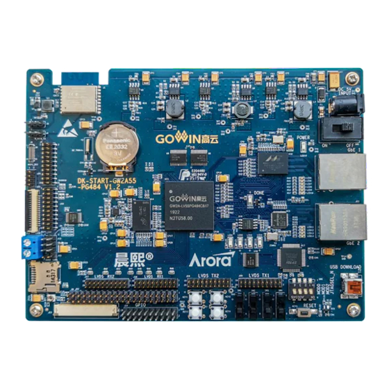
User Manuals: GOWIN DK-START-GW2A55-PG484 V1.3 Board
Manuals and User Guides for GOWIN DK-START-GW2A55-PG484 V1.3 Board. We have
1
GOWIN DK-START-GW2A55-PG484 V1.3 Board manual available for free PDF download: User Manual
GOWIN DK-START-GW2A55-PG484 V1.3 User Manual (44 pages)
Brand:
GOWIN
| Category:
Motherboard
| Size: 2 MB
Table of Contents
Table of Contents
4
List of Figures
7
About this Guide
10
Purpose
10
Related Documents
10
Terminology and Abbreviations
10
Support and Feedback
11
Table 1-1 Abbreviations and Terminology
11
Introduction
12
Overview
12
Figure 2-1 DK-START-GW2A55-PG484_V1.3 Development Board
12
Development Board Suite
13
Figure 2-2 Development Kit
13
PCB Components
14
System Block Diagram
14
Figure 2-3 PCB Components
14
Figure 2-4 System Block Diagram
14
Features
15
Development Board Circuit
17
FPGA Module
17
Download Module
17
Introduction
17
Pinout
18
Figure 3-1 Connection Diagram of FPGA Downloading and Configuration
18
Figure 3-2 Asynchronous FIFO Connection Diagram
18
Table 3-1 FPGA Download and Pinout
18
Power Supply
19
Introduction
19
Table 3-2 Asynchronous FIFO Pinout
19
Clock and Reset
20
Introduction
20
Pinout
20
Figure 3-3 Connection Diagram of Clock and Reset
20
Table 3-3 Clock and Reset Pinout
20
Ddr3
21
Introduction
21
Pinout
21
Figure 3-4 Connection Diagram of FPGA and DDR3
21
Table 3-4 DDR3 Pinout
21
Ethernet
23
Introduction
23
Pinout
23
Figure 3-5 Connection Diagram of FPGA and Ethernet
23
Table 3-5 Ethernet Pinout
23
LVDS Interfaces
24
Introduction
24
Figure 3-6 LVDS TX Interface
24
Pinout
25
Figure 3-7 LVDS RX Interface
25
Table 3-6 LVDS TX Pinout
25
Table 3-7 LVDS TX2 Pinout
25
Mipi Dsi
26
Introduction
26
Table 3-8 LVDS TX2 Pinout
26
Table 3-9 LVDS TX2 Pinout
26
Pinout
27
Figure 3-8 Connection Diagram of MIPI DSI
27
Table 3-10 MIPI DSI Pinout
27
Mipi Csi
28
Introduction
28
Figure 3-9 Connection Diagram of MIPI CSI
28
Pinout
29
SD Card
29
Introduction
29
Figure 3-10 Connection Diagram of SD Card
29
Table 3-11 MIPI DSI Pinout
29
Pinout
30
Rtc
30
Introduction
30
Figure 3-11 Connection Diagram of RTC
30
Table 3-12 SD Card Pinout
30
Table 3-13 RTC Pinout
30
Ad/Da
31
Introduction
31
Pinout
31
Can
31
Figure 3-12 Connection Diagram of AD/DA
31
Table 3-14 AD/DA Pinout
31
Pinout
32
Wifi
32
Introduction
32
Figure 3-13 Connection Diagram of CAN
32
Figure 3-14 Connection Diagram of WIFI
32
Table 3-15 CAN Pinout
32
Table 3-16 WIFI Pinout
32
Gpio
33
Introduction
33
Figure 3-15 40Pin Diagram
33
Pinout
34
Figure 3-16 20Pin Diagram
34
Table 3-17 40Pin Interface Pinout
34
Table 3-18 20Pin Interface Pinout
35
Industry Screen Interface
36
Introduction
36
Figure 3-17 50Pin FPC Interface Diagram
36
Pinout
37
Table 3-19 50Pin FPC Interface Pinout
37
Table 3-20 LCD Screen Brightness Control Pinout
37
LED Module
38
Introduction
38
Pinout
38
Keys Module
38
Figure 3-18 LED Connection Diagram
38
Table 3-21 LED Pinout
38
Pinout
39
Switches Module
39
Introduction
39
Figure 3-19 Key Circuit Diagram
39
Figure 3-20 Switch Circuit Diagram
39
Table 3-22 Keys Module Pinout
39
Pinout
40
Table 3-23 Switches Module Pinout
40
Quick Start
41
Install Software
41
Development Board Power-On Test
41
Build Demo Program
41
Figure 4-1 Design Window
42
Figure 4-2 Process Window
42
Figure 4-3 Build Completed
42
Download and Run
43
Figure 4-4 Programmer Window
43
Figure 4-5 Device Configure Window
43
Figure 4-6 Click Program/Configure
43
Advertisement
Advertisement
Related Products
GOWIN DK-START-GW2A18
GOWIN DK-START-GW2A55-PG484
GOWIN DK-START-GW1NR9
GOWIN DK-GoAI-GW2AR18QN88P
GOWIN DK-START-GW1NS4-QN48
GOWIN DK-START-GW1NR9 V2.1
GOWIN DK-NANO-GW2A55-PG484
GOWIN DK-START-GW1N9
GOWIN DK_START_GW2AR-LV18EQ144PC8I7
GOWIN DK_START_GW2A-LV18PG256C8I7_V2.0
GOWIN Categories
Motherboard
Semiconductors
Computer Hardware
Microcontrollers
Recording Equipment
More GOWIN Manuals
Login
Sign In
OR
Sign in with Facebook
Sign in with Google
Upload manual
Upload from disk
Upload from URL