Table of Contents
Advertisement
Quick Links
AIROC™ CYW20835 Bluetooth® LE system on
chip hardware design guidelines
About this document
This document discusses the hardware design guidelines for the AIROC™ CYW20835 Bluetooth® LE system on
chip kit.
Scope and purpose
This document provides basic guidelines on layout for AIROC™ CYW20835 Bluetooth® LE system on chip.
Intended audience
This document provides hardware guidance on how to design with CYW20835.
User Guide
Please read the Important Notice and Warnings at the end of this document
002-34024 Rev. **
www.infineon.com
page 1 of 11
2021-10-05
Advertisement
Table of Contents

Related Manuals for Infineon AIROC CYW20835


Summary of Contents for Infineon AIROC CYW20835
-
Page 1: About This Document
This document provides basic guidelines on layout for AIROC™ CYW20835 Bluetooth® LE system on chip. Intended audience This document provides hardware guidance on how to design with CYW20835. User Guide Please read the Important Notice and Warnings at the end of this document 002-34024 Rev. ** www.infineon.com page 1 of 11 2021-10-05... -
Page 2: Table Of Contents
AIROC™ CYW20835 Bluetooth® LE system on chip hardware design guidelines Table of contents Table of contents About this document ........................1 Table of contents ..........................2 Basic layout guidelines ......................3 Component placement ......................4 Antenna placement ..........................4 PCB antenna ............................4 Crystal placement ........................... -
Page 3: Basic Layout Guidelines
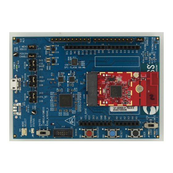
AIROC™ CYW20835 Bluetooth® LE system on chip hardware design guidelines Basic layout guidelines Basic layout guidelines Most Bluetooth® devices use four‐layer boards to minimize thickness. Components are placed on the top layer; the bottom layer is a solid ground fill. Most signal traces are routed on the top layer. For RF traces, use a 50‐ohm transmission line to minimize mismatch losses and reflections, and therefore maximize the power transferred to the load. -
Page 4: Component Placement
AIROC™ CYW20835 Bluetooth® LE system on chip hardware design guidelines Component placement Component placement As a rule, follow the receive signal flow from the antenna to the antenna matching and filter circuits, then to the low-noise amplifier (LNA) chip input. Keep the radio front end (RF), power management unit (PMU), and baseband (BB) decoupling capacitors next to CYW20835 pin pads. -
Page 5: Decoupling Capacitors
Component placement Decoupling capacitors See the reference schematic for decoupling capacitor usage and values on different power domains. Infineon recommends that you use the vendor and part numbers shown in the reference design BOM. Decoupling capacitors must be placed as close to its associated pin as possible. -
Page 6: Serial Flash
AIROC™ CYW20835 Bluetooth® LE system on chip hardware design guidelines Component placement Serial flash The CYW20835 kit uses the GD25WD80C serial flash from GigaDevice. Place the flash device on the same side as pins 35–40 of the CYW20835 device so that serial flash signals are relatively short; this helps to minimize unnecessary crossing with other signals. -
Page 7: Power Inductor
AIROC™ CYW20835 Bluetooth® LE system on chip hardware design guidelines Component placement VDDIO to LHL_VDDO (pin 60)/BT_VDDO (pin 36) → Minimum 8 mils trace width − BT_VDDC → Minimum 10 mils trace width − BT_VDDC (pin 37) → Minimum 8 mils trace width −... -
Page 8: Layer 4
AIROC™ CYW20835 Bluetooth® LE system on chip hardware design guidelines Component placement Figure 6 Power inductor routing 2.13 Layer 4 Use Layer 4 for all non-critical signal routing. Figure 7 Layer 4 User Guide 8 of 11 002-34024 Rev. ** 2021-10-05... -
Page 9: Assembly Instructions
AIROC™ CYW20835 Bluetooth® LE system on chip hardware design guidelines Component placement 2.14 Assembly instructions CYW20835 is an Infineon standard QFN (quad flat no-lead) package. For additional assembly instructions and reflow profiles, see AN72845 - Design guidelines for quad flat no-lead (QFN) packaged devices. User Guide 9 of 11 002-34024 Rev. -
Page 10: Revision History
AIROC™ CYW20835 Bluetooth® LE system on chip hardware design guidelines Revision history Revision history Major changes since the last revision Date Version Description 2021-10-05 Initial release. User Guide 10 of 11 002-34024 Rev. ** 2021-10-05... - Page 11 With respect to any examples, hints or any typical WARNINGS values stated herein and/or any information 81726 Munich, Germany regarding the application of the product, Infineon Due to technical requirements products may contain Technologies hereby disclaims any and all dangerous substances. For information on the types...
Need help?
Do you have a question about the AIROC CYW20835 and is the answer not in the manual?
Questions and answers