Table of Contents
Advertisement
Quick Links
Introduction
This user guide introduces the evaluation kits for the Atmel
embedded MPUs listed below:
SAMA5D31
SAMA5D33
SAMA5D34
SAMA5D35
SAMA5D36
It pertains to the following evaluation kit references:
SAMA5D31-EK
SAMA5D33-EK
SAMA5D34-EK
SAMA5D35-EK
SAMA5D36-EK
ARM-based Embedded MPUs
SAMA5D3x-EK User Guide
USER GUIDE
®
SAMA5D3 series
11180B–ATARM–29-Oct-13
Advertisement
Table of Contents

Related Manuals for Atmel SAMA5D3 EK Series


Summary of Contents for Atmel SAMA5D3 EK Series
-
Page 1: Introduction
ARM-based Embedded MPUs SAMA5D3x-EK User Guide USER GUIDE Introduction ® This user guide introduces the evaluation kits for the Atmel SAMA5D3 series embedded MPUs listed below: SAMA5D31 SAMA5D33 SAMA5D34 SAMA5D35 SAMA5D36 It pertains to the following evaluation kit references: ... -
Page 2: Contents
One universal input AC/DC power supply with US, Europe and UK plug adapters One 3V lithium battery type CR1225 Cables One micro A/B-type USB cable One RJ45 crossed cable A welcome letter Related Items Atmel SAMA5D3 Series Datasheet SAMA5D3x-EK User Guide [USER GUIDE] 11180B–ATARM–29-Oct-13... -
Page 3: Table Of Contents
Table of Contents Introduction ..........1 Contents . -
Page 4: Evaluation Kit Specifications
Evaluation Kit Specifications Table 1-1. Evaluation Kit Specifications Characteristic Specifications Clock speed Up to 536 MHz PCK, up to 166 MHz MCK Ports 10/100/1000 Ethernet, USB, RS232, JTAG, CAN, Audio, HDMI, SD card Board supply voltage 5V DC from connector Dimensions: MB (Main Board) 165 * 135 * 20 mm... -
Page 5: Power Up
After booting up the board, you can run sample code or your own application on the development kit. You can download sample code and get technical support from the Atmel web site. Linux software and demos can be found on the web site Linux4SAM. -
Page 6: Evaluation Kit Hardware
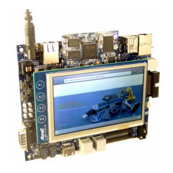
The evaluation kit allows users to extensively evaluate, prototype and create application-specific designs. The Atmel SAMA5D3 series evaluation kit is a platform architecture based on a main board, a computer module equipped with a SAMA5D3 series processor and an optional display module, providing maximum flexibility for kit users. -
Page 7: Cpu Module (Cm) Board
CPU Module (CM) Board Overview The CPU module (CM) board is the heart of the SAMA5D3x-EK. It connects to the main board through a SODIMM200 interface and integrates the SAMA5D3 series processor and external memories. The CM board serves as a minimal CPU sub-system. - Page 8 Figure 4-1. CPU Module Board from Embest/Flextronics Figure 4-2. CPU Module Board from Ronetix SAMA5D3x-EK User Guide [USER GUIDE] 11180B–ATARM–29-Oct-13...
- Page 9 Figure 4-3. Board Architecture Nand Flash Nand Flash Nand Flash N N a a n n d d F F l l a a s s h h Nand Flash Nand Flash Nand Flash Nand Flash Nand Flash Nand Flash Nand Flash Nand Flash Nand Flash...
-
Page 10: Equipment List
Equipment List ® ® The CM board is built around an ARM Cortex -A5-based microcontroller (BGA 324 package) with external memory and Gigabit Ethernet PHYsical layer transceiver. 4.2.1 Devices Table 4-2. CPU Module Specifications Characteristic Specifications CPU Module (10 layers) Dimensions in mm: (L x W x H) 67.60 *(40 to 47) * 5 max... - Page 11 4.2.4 Boot Options Table 4-3 lists the supported boot options Table 4-3. Boot Options Boot Mode Boot Device Type Note BMS OPEN Embedded ROM Boot ROM Boot followed by: Default boot is from embedded ROM - SPI0, NPCS0 - SD/MMC MCI0, MCI1 - NAND Flash - SPI0, NPCS1 - TWI0...
-
Page 12: Functional Blocks
Functional Blocks 4.3.1 Processor The CM board is equipped with one Atmel SAMA5D3 ARM-based embedded MPU from the list below: SAMA5D31 SAMA5D33 SAMA5D34 SAMA5D35 SAMA5D36 The SAMA5D3x devices are packaged in a BGA324-ball BGA package and share an identical footprint. - Page 13 4.3.4 Power Supplies The CM board is driven by +3.3V input power rail from the MB through the SODIMM200 connector. The CM board embeds all necessary power rails required for the microprocessor. When additional voltages are required, they are generated on-board from the 3.3V supply (power source is a linear regulator or a switching regulator).
- Page 14 Figure 4-4. Embest/Flextronics Power Supply VCC_3V3 VDDIOP1 180ohm at 100MHz 180ohm at 100MHz VCC_1V2 MN15 MN15 RT9018B-18GSP RT9018B-18GSP VCC_3V3 NTRST 100nF 100nF 100nF 100nF 180ohm at 100MHz 180ohm at 100MHz VOUT C131 C131 C132 C132 C134 C134 100nF 100nF 10uF 10uF 10uF 10uF...
- Page 15 Figure 4-5. Ronetix Power Supply Soft-Start Time EN Input High Threshold EN Input Low Threshold SEE TABLE 1 VDD_CORE LQM2HPN1R0MG0L 22u/6V3 22u/6V3 VOUT 0402 100k SC189ASKTRT 1V0 2k49/1% 10k/1% POWER_ENABLE SEE TABLE 1 GND pins are provided and should be VDDIODDR LQM2HPN1R0MG0L 22u/6V3...
- Page 16 Figure 4-6. Ronetix Power Supply (Continued) (3V3) VDD_IOM VDD_IOP0 VDD_IOP1 VDD_CORE U3-A 100n/10V 100n/10V VDDIOM VDDCORE 100n/10V 100n/10V VDDIOM VDDCORE 100n/10V VDDCORE 100n/10V GNDIOM VDDCORE 100n/10V GNDIOM VDDCORE 100n/10V VDDCORE 100n/10V 100n/10V VDDIOP0 VDDCORE 100n/10V VDDIOP0 100n/10V VDDIOP1 GNDCORE 100n/10V VDDIOP1 GNDCORE GNDCORE...
- Page 17 4.3.5 Memory 4.3.5.1 Memory Organization The SAMA5D3 series processor features a DDR/SDR memory interface and an External Bus Interface (EBI) to interface to a wide range of external memories and to almost any kind of parallel peripheral. 4.3.5.2 Resource Allocation This section describes the memory devices that equip the SAMA5D3 series CM board.
- Page 18 Figure 4-8. Ronetix DDR2 Memory DDR_ADDR Address and control traces may not exceed 1.3 inches (33.0 mm). U3-H 12.09.2012 Address and control traces must be length-matched to within 0.1 inch (2.54 mm). DDR_A0 DDR_A[0-13] Chenged U4 and U5 DDR_A0 Address and control traces must match the data group trace lengths to within 0.25 inches (6.35 mm). DDR_A1 From MT47H64M16HR-25H to MT47H128M16RT-3:C DDR_A1...
- Page 19 Figure 4-9. Embest/Flextronics External Memory JS28F128P33TF70A JS28F128P33TF70A FLASH_A1 M_EBI_D0 FLASH_A2 M_EBI_D1 FLASH_A3 M_EBI_D2 FLASH_A4 M_EBI_D3 FLASH_A5 M_EBI_D4 FLASH_A6 M_EBI_D5 FLASH_A7 M_EBI_D6 FLASH_A8 M_EBI_D7 FLASH_A9 M_EBI_D8 FLASH_A10 M_EBI_D9 FLASH_A11 M_EBI_D10 DQ10 FLASH_A12 M_EBI_D11 DQ11 FLASH_A13 M_EBI_D12 DQ12 FLASH_A14 M_EBI_D13 DQ13 FLASH_A15 M_EBI_D14 DQ14 FLASH_A16...
- Page 20 Figure 4-10. Ronetix External Memory U3-G PE0/A0(NBS0) A1_NOR PE1/A1 A2_NOR PE2/A2 A3_NOR VDD_IOM PE3/A3 A4_NOR PE4/A4 A5_NOR PE5/A5 A6_NOR PE6/A6 NOR FLASH A7_NOR PE7/A7 A8_NOR 100k PE8/A8 A9_NOR PE9/A9 A10_NOR PE26/NCS0/TXD2 PE10/A10 0402 A11_NOR NWE_NOR/NAND_WE PE11/A11 A12_NOR NRD_NOR/NAND_OE PE12/A12 A13_NOR NRST PE13/A13 2;7;8...
- Page 21 4.3.6 Serial Peripheral Interface Controller (SPI) The SAMA5D3 series processor provides two high-speed Serial Peripheral Interface (SPI) controllers. One port is used to interface with the on-board serial DataFlash. Note that the on-board serial DataFlash is enabled through a jumper: JP1 on Embest modules, J1 on Ronetix modules.
- Page 22 4.3.7 1-Wire EEPROM The SAMA5D3 series CM board uses a 1-wire device as a “soft label” to store information such as chip type, manufacture name, production date, etc. Only page 1 is used. Warning: Do not modify the information contained in this page. Pages 2 to n remain free for the user.
- Page 23 4.3.8 Tri-Speed Ethernet PHY The SAMA5D3 series CM board is equipped with a MICREL PHY device (MICREL KSZ9021/31) operating at 10/100/1000 Mbps. The board supports the RGMII interface mode. The Ethernet interface consists of four pairs of low- voltage differential pair signals designated from GRX± and GTx± plus control signals for link activity indicators. These signals can be used to connect to a 10/100/1000 Base-T RJ45 connector integrated on the main board.
- Page 24 Figure 4-16. Ronetix GEthernet ETH0 ETH_DVDDL 2A ! max 345mA--> BLM21PG221SN1D C128 22u/6V3 22u/6V3 ETH_AVDDL 2A ! max 205mA--> BLM21PG221SN1D C129 ETH_AVDDH VDD_IOP1 22u/6V3 22u/6V3 max ?mA--> ETH_AVDDL_PLL 2A ! 0.5A ! max ?mA--> max 563mA--> ETH_V1 max 13mA--> BLM21PG221SN1D LQM2HPN1R0MG0L BLM15AG121SN1D C131...
- Page 25 4.3.9 Indicators There are two LEDs on the SAMA5D3 series CM board that can be controlled by the user. Both are controlled by GPIO lines PE24 and PE25 as shown below. Figure 4-17. Embest/Flextronics LED Indicators VCC_3V3 {3,7} PE[23..31] Blue Blue 470R 470R...
- Page 26 4.3.10 SODIMM200 Interface The SAMA5D3 series CM board uses SODIMM200 card edge connector to interface with the MB board. Refer to Section 5.4.22 “SODIMM Card Edge Socket”. 4.3.11 Connectors Figure 4-19 shows the mechanical dimensions of the SAMA5D3 series CM board outline and the mounting holes. Figure 4-19.
-
Page 27: Embest/Flextronics Schematics
Embest/Flextronics Schematics This SAMA5D3x-EK CM board manufactured by Embest/Flextronics is available in Revision D and Revision E. In this section, schematics are provided for both revisions. 4.4.1 CPU Module Revision D Schematics This section contains the following schematics: Block diagram ... - Page 28 3V3 INPUT VBAT ANALOG Reference ATMEL USB A,B,C SAMA5D3 SERIES ARM CORTEX A5-BASED PROCESSOR PIO A,...E PIO A,... PIO A&D PIO B&E SERIAL ONE WIRE SERIAL DATA EEPROM EEPROM FLASH PIO C...
- Page 29 VCC_3V3 VDDIOP1 180ohm at 100MHz 180ohm at 100MHz VCC_1V2 NTRST 100nF 100nF 100nF 100nF 180ohm at 100MHz 180ohm at 100MHz C131 C131 100nF 100nF C0603 C0603 VDDBU VDDIOP0 100nF 100nF 100nF 100nF 100nF 100nF 100nF 100nF 100nF 100nF 100nF 100nF 100nF 100nF 100nF...
- Page 30 MN2E MN2E M_EBI_A0 TP21 TP21 MN2F MN2F SAMA5D3x_BGA324 SAMA5D3x_BGA324 SAMA5D3x_BGA324 SAMA5D3x_BGA324 DDR_A[0..13] PE0_A0/NBS0 FLASH_A1 PE1_A1 DDR_A0 FLASH_A2 DDR_A0 PE2_A2 DDR_A1 FLASH_A3 DDR_A1 PE3_A3 DDR_A2 FLASH_A4 DDR_A2 PE4_A4 DDR_A3 FLASH_A5 DDR_A3 PE5_A5 DDR_A4 FLASH_A6 DDR_A4 PE6_A6 DDR_A5 FLASH_A7 DDR_A5 PE7_A7 DDR_A6 FLASH_A8 DDR_A6 PE8_A8...
- Page 31 DDR_D[0..31] DDR_A[0..13] DDR_A0 DDR_D0 DDR_A0 DDR_A1 DDR2 SDRAM DDR2 SDRAM DDR_D1 DDR_A1 DDR2 SD DDR2 SD DDR_A2 DDR_D2 DDR_A2 MT47H128M16RT MT47H128M16RT MT47H128M MT47H128M DDR_A3 DDR_D3 DDR_A3 DDR_A4 DDR_D4 DDR_A4 DDR_A5 DDR_D5 DDR_A5 DDR_A6 DDR_D6 DDR_A6 DDR_A7 DDR_D7 DDR_A7 DDR_A8 DDR_D8 DDR_A8 DDR_A9 DDR_D9...
- Page 32 PA[0..31] {7} PC[0..31] {7} MN2A MN2A MN2C MN2C PD11 SAMA5D3x_BGA324 SAMA5D3x_BGA324 SAMA5D3x_BGA324 SAMA5D3x_BGA324 PD10 PD12 PA0_LCDDAT0 PC0_ETX0 PA1_LCDDAT1 PC1_ETX1 PA2_LCDDAT2 PC2_ERX0 PA3_LCDDAT3 PC3_ERX1 PA4_LCDDAT4 PC4_ETXEN PA5_LCDDAT5 PC5_ECRSDV PA6_LCDDAT6 PC6_ERXER PA7_LCDDAT7 PC7_EREFCK VDDIOP1 PA8_LCDDAT8 PC8_EMDC PA9_LCDDAT9 PC9_EMDIO PA10 PC10 PA10_LCDDAT10 PC10 PA11 PC11 PA11_LCDDAT11...
- Page 33 AVDDL_PLL 10nF 10nF 10nF 10nF 10uF 10uF 4.7K 4.7K VDDIOP1 G125C INT_G VDDIOP1 180ohm at 100MHz 180ohm at 100MHz AVDDH GMDIO VDDIOP1 10nF 10nF 10nF 10nF 10nF 10nF 10uF 10uF 4.99K 1% 4.99K 1% C100 C100 C101 C101 C102 C102 C103 C103 10nF...
- Page 34 VCC_5V VCC_5V VCC_5V_1 VCC_5V_2 VDDBU VCC_5V_3 VCC_5V_4 GND1 VBAT PE23 PE29 PA[0..31] PE23 PE29 C122 C122 PE24 PE30 PE24 PE30 PE25 PE31 PE25 PE31 PE26 VDDIOM PE26 GND2 VDDIOM VDDIOM_1 VDDIOM_2 PC25 PC24 PC25 PC24 PC23 PC22 C123 C123 PC23 PC22 PC21 PC20...
- Page 35 4.4.2 CPU Module Revision E Schematics This section contains the following schematics: Main sheet SODIMM 200 Power supply CPU power supply DDR2 interface FI: NAND, NOR, Serial, I2C, 1-wire Ethernet USB, JTAG, LEDs ...
- Page 36 3V3 INPUT VBAT ANALOG Reference ATMEL USB A,B,C ARMA5 PROCESSOR ATSAMA5D3x-CU PIO A,...E PIO A,... PIO A&D PIO B&E SERIAL ONE WIRE DATA TWO LED EEPROM FLASH PIO C...
- Page 37 TP17 VCC_3V3 VDDIOP1 180ohm at 100MHz VCC_1V2 NTRST TP11 100nF 100nF 180ohm at 100MHz TP14 100nF VDDBU VDDIOP0 VDDIOP0 TP21 TP16 TP13 100nF 100nF 100nF 100nF 100nF 100nF 100nF 100nF C101 100nF 100nF 4.7uF NRST VDDBU VDDIODDR 100nF 10uF VDDIOM JTAGSEL JTAGSEL VDDIOM_1...
- Page 38 MN4E M_EBI_A0 MN4F ATSAMA5D3x-CU ATSAMA5D3x-CU DDR_A[0..13] PE0_A0/NBS0 FLASH_A1 PE1_A1 DDR_A0 FLASH_A2 DDR_A0 PE2_A2 DDR_A1 FLASH_A3 DDR_A1 PE3_A3 DDR_A2 FLASH_A4 DDR_A2 PE4_A4 DDR_A3 FLASH_A5 DDR_A3 PE5_A5 DDR_A4 FLASH_A6 DDR_A4 PE6_A6 DDR_A5 FLASH_A7 DDR_A5 PE7_A7 DDR_A6 FLASH_A8 DDR_A6 PE8_A8 DDR_A7 FLASH_A9 DDR_A7 PE9_A9 DDR_A8 FLASH_A10...
- Page 39 PA[0..31] {7} PC[0..31] {7} MN4A MN4C PD11 ATSAMA5D3x-CU ATSAMA5D3x-CU PD10 PD12 PA0_LCDDAT0 PC0_ETX0 PA1_LCDDAT1 PC1_ETX1 PA2_LCDDAT2 PC2_ERX0 PA3_LCDDAT3 PC3_ERX1 PA4_LCDDAT4 PC4_ETXEN PA5_LCDDAT5 PC5_ECRSDV PA6_LCDDAT6 PC6_ERXER PA7_LCDDAT7 PC7_EREFCK VDDIOP1 PA8_LCDDAT8 PC8_EMDC PA9_LCDDAT9 PC9_EMDIO PA10 PC10 PA10_LCDDAT10 PC10 PA11 PC11 PA11_LCDDAT11 PC11 PA12 PC12 PA12_LCDDAT12...
- Page 40 DDR_D[0..31] DDR_A[0..13] DDR_A0 DDR_D0 DDR_A0 DDR_A1 DDR2 SDRAM DDR_D1 DDR_A1 DDR2 SDR DDR_A2 DDR_D2 DDR_A2 MT47H128M16RT MT47H128M DDR_A3 DDR_D3 DDR_A3 DDR_A4 DDR_D4 DDR_A4 DDR_A5 DDR_D5 DDR_A5 DDR_A6 DDR_D6 DDR_A6 DDR_A7 DDR_D7 DDR_A7 DDR_A8 DDR_D8 DDR_A8 DDR_A9 DDR_D9 DDR_A9 DDR_A10 DDR_D10 DDR_A10 DQ10 DDR_A11...
- Page 41 AVDDL_PLL C109 C112 C125 10nF 10nF 10uF 4.7K VDDIOP1 G125C INT_G VDDIOP1 180ohm at 100MHz AVDDH GMDIO VDDIOP1 C115 C122 C118 C121 10nF 10nF 10nF 10uF 4.99K 1% C105 C111 10nF 10nF 10nF 10uF AVDDL KSZ9021RNI VDDIOP1 C124 C120 C119 10nF 10nF 10uF...
- Page 42 VCC_5V VCC_5V VCC_5V_1 VCC_5V_2 VDDBU VCC_5V_3 VCC_5V_4 GND1 VBAT PE23 PE29 PA[0..31] PE23 PE29 PE24 PE30 PE24 PE30 PE25 PE31 PE25 PE31 PE26 VDDIOM PE26 GND2 VDDIOM VDDIOM_1 VDDIOM_2 PC25 PC24 PC25 PC24 PC23 PC22 PC23 PC22 PC21 PC20 4.7uF PC21 PC20 PC19...
-
Page 43: Ronetix Schematics
Ronetix Schematics This section contains the schematics for the CM board manufactured by Ronetix: Main sheet SODIMM200 Power supply CPU power supply DDR2 interface FI: NAND, NOR, Serial, I2C, 1-wire Ethernet USB, JTAG, LEDs ... - Page 44 SCHEMATICS: SAMA5D3x-CM SHEET # SHEET NAME DATE: DESCRIPTION MAIN SAMA5D3x-CM v2.0 15.03.2012 SODIM200 SAMA5D3x-CM v2.0 20.09.2012 POWER SUPPLY Changes Rev2.0 CPU-POWER SUPPLY 1. SoDIMM200 change: * PB13 pin 144 with 0R DNP * PB12 pin 146 with 0R populated DDR2 INTERFACE 2.
- Page 45 PE24/RTS2 PE30/NWAIT PE25/RXD2/1-Wire PE31/IRQ/PWML1 PE26/NCS0/TXD2 VDD_IOM VDD_IOM PC25/SPI1_NPCS0 PC24/SPI1_SPCK PC23/SPI1_MOSI PC22/SPI1_MISO PC21/RD0 PC20/RF0 PC19/RK0 PC18/TD0 PC17/TF0 PC16/TK0 PC9/EMDIO PC8/EMDC/TCLK5 PC7/EREFCK/TIOB5 PC6/ERXER/TIOA5 PC4/ETXEN/TIOB4 PC5/ECRSDV/TCLK4 PC2/ERX0/TCLK3 PC3/ERX1/TIOA4 PC0/ETX0/TIOA3 PC1/ETX1/TIOB3 POWER_ENABLE Enable_0 Enable_1 CS_BOOT_DISABLE 100n/10V 100n/10V Enable_2 Enable_3 ADVREF PE27/NCS1/TIOA2/LCDDAT22 PE28/NCS2/TIOB2/LCDDAT23 PC10/MCI2_CDA//LCDDAT20 PC11/MCI2_DA0//LCDDAT19 PC13/MCI2_DA2/TIOB1/LCDDAT17 PC12/MCI2_DA1/TIOA1/LCDDAT18 PC15/MCI2_CK/PCK2/LCDDAT21...
- Page 46 Soft-Start Time EN Input High Threshold EN Input Low Threshold SEE TABLE 1 VDD_CORE LQM2HPN1R0MG0L 22u/6V3 22u/6V3 VOUT 0402 100k SC189ASKTRT 1V0 2k49/1% 10k/1% POWER_ENABLE SEE TABLE 1 VDDIODDR LQM2HPN1R0MG0L 22u/6V3 R3 5k1/1% 22u/6V3 VOUT 0402 SC189ASKTRT 1V0 6k34/1% VDDFUSE MCP1700T-2502E/TT Out 1 VDD_CORE...
- Page 47 (3V3) VDD_IOM VDD_IOP0 VDD_IOP1 VDD_CORE U3-A 100n/10V 100n/10V VDDIOM VDDCORE 100n/10V 100n/10V VDDIOM VDDCORE 100n/10V VDDCORE 100n/10V GNDIOM VDDCORE 100n/10V GNDIOM VDDCORE 100n/10V VDDCORE 100n/10V 100n/10V VDDIOP0 VDDCORE 100n/10V VDDIOP0 100n/10V VDDIOP1 GNDCORE 100n/10V VDDIOP1 GNDCORE GNDCORE GNDIOP GNDCORE GNDIOP GNDCORE VDDIODDR GNDIOP...
- Page 48 DDR_ADDR Address and control traces may not exceed 1.3 inches (33.0 mm). U3-H Address and control traces must be length-matched to within 0.1 inch (2.54 mm). DDR_A0 DDR_A[0-13] DDR_A0 Address and control traces must match the data group trace lengths to within 0.25 inches (6.35 mm). DDR_A1 DDR_A1 DDR_A2...
- Page 49 A1_NOR PE1/A1 A2_NOR PE2/A2 A3_NOR VDD_I PE3/A3 A4_NOR PE4/A4 A5_NOR PE5/A5 A6_NOR PE6/A6 NOR FLASH A7_NOR PE7/A7 L3 & L8 A8_NOR PE8/A8 Zo=60 ohms +/-10% A9_NOR PE9/A9 A10_NOR PE10/A10 A11_NOR PE11/A11 A12_NOR PE12/A12 A13_NOR PE13/A13 A14_NOR PE14/A14 BYTE# A15_NOR PE15/A15/SCK3 R/B# A16_NOR PE16/A16/CTS3...
- Page 50 ETH_AVDDH VDD_IOP1 max ?mA--> 2A ! max ?mA--> max 563mA--> ETH_V1 BLM21PG221SN1D LQM2HPN1R0MG0L C131 C106 C107 22u/6V3 VOUT 0402 10n/25V 100n/10V SC189ASKTRT 1V0 C127 2k/1% 10k/1% ETH_DVDDH GND GND 2A ! max ?mA--> BLM21PG221SN1D C132 22u/6V3 22u/6V3 PB0/GTX0 PB1/GTX1 PB2/GTX2 place close to CPU U3-D PB3/GTX3...
- Page 51 SOFT MODEM Cl=Cs+[C1xC2]/[C1+C2] if C1=C2 => C100 C1,2=2[Cl-Cs] !!! U3-B Cl is load capacitance of the cristal 27p/50V top/bot CS is the stray capacitance on the printed circuit board, typically a value of 5pf can be used for calculation top/bot CPX32-12.000MHz XOUT C101...
- Page 52 PA4/LCDDAT4 PA4/LCDDAT4 PA5/LCDDAT5 PA5/LCDDAT5 PA6/LCDDAT6 PA6/LCDDAT6 PA7/LCDDAT7 PA7/LCDDAT7 PA8/LCDDAT8 PA8/LCDDAT8 PA9/LCDDAT9 PA9/LCDDAT9 PA10/LCDDAT10 PA10/LCDDAT10 PA11/LCDDAT11 PA11/LCDDAT11 PA12/LCDDAT12 PA12/LCDDAT12 PA13/LCDDAT13 PA13/LCDDAT13 PA14/LCDDAT14 PA14/LCDDAT14 PA15/LCDDAT15 PA15/LCDDAT15 PA16/LCDDAT16/ISI_D0 PA16/LCDDAT16/ISI_D0 PA17/LCDDAT17/ISI_D1 PA17/LCDDAT17/ISI_D1 PA18/LCDDAT18/TWD2/ISI_D2 PA18/LCDDAT18/TWD2/ISI_D2 PA19/LCDDAT19/TWCK2/ISI_D3 PA19/LCDDAT19/TWCK2/ISI_D3 PA20/LCDDAT20/PWMH0 PA20/LCDDAT20/PWMH0 PA21/LCDDAT21/PWML0/ISI_D5 PA21/LCDDAT21/PWML0/ISI_D5 PA22/LCDDAT22/PWMH1 PA22/LCDDAT22/PWMH1 PA23/LCDDAT23/PWML1/ISI_D7 PA23/LCDDAT23/PWML1/ISI_D7 PA24/LCDPWM PA24/LCDPWM PA25/LCDDISP...
-
Page 53: Main Board (Mb)
Main Board (MB) Main Board Overview The SAMA5D3 series main board (MB) hosts any of the SAMA5D31/33/34/35/36 CPU module boards (CM). The main board features all necessary peripheral devices and interfaces for processor evaluation. Figure 5-1. Main Board Top View SAMA5D3x-EK User Guide [USER GUIDE] 11180B–ATARM–29-Oct-13... - Page 54 Figure 5-2. Annotated MB Layout SAMA5D3x-EK User Guide [USER GUIDE] 11180B–ATARM–29-Oct-13...
- Page 55 5.1.1 Equipment List The SAMA5D3 series MB is a full-featured motherboard. It can be used with all available SAMA5D3 series CM boards. 5.1.2 Technical Specifications Table 5-1. MB Technical Specifications Characteristic Specifications Supported Module All SAMA5D3 series computer modules Expansion Slots One 200-pin SODIMM socket Mass Storage Interface Two high-speed memory card hosts...
- Page 56 5.1.3 Devices List of the MB board peripherals: Two EMAC PHY One audio CODEC Two high-speed MCI card interfaces Two CAN transceivers One RS232 port with level translator features USART1 One Smart DAA port ...
- Page 57 Figure 5-3. MB Architecture COM1 or COM1 or On Board JTAG On Board JTAG VCC 5V Jack VCC 5V Jack Audio Audio Audio Audio MIC1 MIC1 MCI0 MCI0 CAN0 & 1 CAN0 & 1 DBGU DBGU Bridge Bridge ZIGBEE ZIGBEE Modem Modem RS232...
-
Page 58: Function Blocks
Function Blocks 5.2.1 Processor The SAMA5D3 series MB board may be used with any of the SAMA5D31/D33/D34/D35/SAMA5D36 CPU modules. Figure 5-4. SODIMM Interface on MB VDDIOP0 JP9 for BMS Config: When Open,BMS=1: Boot on embeded ROM When Close,BMS=0: Boot on External memory 4.7k 4.7k VCC5V_1... - Page 59 5.2.2 Power Supplies The SAMA5D3 series MB is supplied with a simple external 5 VCC power supply. The MB features one adjustable low- dropout regulator (LDO). It accepts DC in 5V power and outputs a regulated +3.3V to most other circuits on the board through four 3.3V rails.
- Page 60 5.2.3 Debug JTAG/ICE and DBGU The MB includes a built-in SEGGER J-Link-on-Board device. The functionality is implemented with an ATSAM3U4C microcontroller in an LQFP100 package. The ATSAM3U4C provides the functions of JTAG and a bridge USB/Serial DBGU port. Two LEDs D13 and D14 that are mounted on the main board signal the status of the J-Link-on-Board device. The J-Link-OB-ATSAM3U4C was designed in order to provide an efficient, on-board alternative to the general J-Link.
- Page 61 5.2.3.1 Disabling J-Link-OB-ATSAM3U4C Jumper JP15 disables the J-Link-OB-ATSAM3U4C JTAG functionality. When the jumper is installed, it grounds Pin 25 of the ATSAM3U4C that is normally pulled high. This signals to the microcontroller it must not provide JTAG support. Jumper JP15 not installed: J-Link-OB-ATSAM3U4C is enabled and fully functional ...
- Page 62 All three USB host ports are equipped with 500 mA high-side power switch for self-powered and bus-powered applications. The USB device port feature VBUS insert detection function through the resistor ladder R138 and R139. Refer to the embedded MPU product datasheet for detailed programming information, available on www.atmel.com. Figure 5-8.
- Page 63 5.2.6 Ethernet 10/100 (EMAC) Port The main board contains a MICREL PHY device (KSZ8051) handling Ethernet connectivity at 10/100 Mbps. The device supports MII and RMII interface modes. There are two independent PHY devices placed on CM and MB boards that connect to two separate RJ-45 connectors and that contain built-in magnetics and status LEDs.
- Page 64 Figure 5-11. ETH1 Port ETH1 VDDIOP0 C122 C122 100n 100n 10Base-T/100Base-TX GND_ETH1 C100 C100 220ohm at 100MHz 220ohm at 100MHz R136 R136 R170 R170 R162 R162 49.9R 49.9R 49.9R 49.9R EARTH_ETH1 EARTH_ETH1 GND_ETH1 RR17 RR17 MN20 MN20 REF_CLK/B-CAST_OFF E1_TXCK T D + T D + T X + T X +...
- Page 65 5.2.7 Audio The MB includes a WM8904 CODEC that provides route to handle audio in the digital domain. The interface includes audio jacks for line input (J13) and headphone line output (J15). It also connects to an electret microphone, which is conveniently installed on the main board.
- Page 66 5.2.8 HDMI Transmitter Interface The Main Board (MB) is equipped with an HDMI transmitter interface. The SiI9022/9024 HDMI Tx provides a complete solution for transmitting HDMI compliant digital audio/video. Specialized audio/video processing is available within the transmitter to easily and cost-effectively add HDMI capability to consumer electronics devices.
- Page 67 5.2.9 1-Wire EEPROM The MB also features a 1-wire device as a “software identification label” to store information such as chip type, manufacture name, production date, etc. Figure 5-14. 1-Wire on MB ONE WIRE EEPROM R144 R144 1.5k 1.5k MN16 MN16 N E _ W I R E PE25...
- Page 68 5.2.11 Smart DAA The SAMA5D3 series MB features a Smart DAA chip to drive an analog telephone line on RJ11 6P4C port (J16). Figure 5-16. Smart DAA 220ohm at 100MHz 220ohm at 100MHz 6.81M 6.81M MN11 MN11 MMBD3004S-7-F MMBD3004S-7-F TEST 470p 470p RJ11...
- Page 69 5.2.12 SD/MMC Interface SD/MMC is a standard Secure Digital/MultiMedia Card interface. The MB has two high-speed Multimedia Card Interfaces (MCI). The first interface is used as an 8-bit interface (MCI0), connected to an SD/MMC card slot. The second interface is used as a 4-bit interface (MCI1), connected to a MicroSD card slot. Each power line is on by default and is connected to a MOSFET controlled by a PIO to switch on or off the SD card power.
- Page 70 5.2.13 ZigBee The MB has a 10-pin male connector for the Atmel RZ600 ZigBee module. Not populated (DNP) 0 Ohm resistors have been implemented in series with the PIO lines that are used elsewhere in the design This ensures that in case of a conflict in the user application, the lines can be disconnected individually.
- Page 71 5.2.15.2 CS_BOOT Button The CS_BOOT can be used to prevent the system from booting out of external memories (NANDFlash, SPI Flash). The purpose is mainly to execute the SAM-BA part of the ROM code. Two methods can be used: Press the CS_BOOT and power-cycle the board. Press the CS_BOOT and then press the NRST button.
- Page 72 5.2.17 Expansion Ports Three 40-pin headers (J1, J2, J3) are provided on the board to allow for the PIO connection of various expansion cards that could be developed by the users or other sources. Due to multiplexing, different signals can be provided on each pin. Figure 5-21.
- Page 73 Figure 5-22. LCD Expansion R147 R147 R148 R148 Z B _ I R Q 0 Z B _ I R Q 1 PE30 10,3,6 PE31 R146 R146 R149 R149 T W C K 1 ( S P I 1 _ N P C S 2 ) T W D 1 ( S P I 1 _ N P C S 1 ) 13,3 PC26...
-
Page 74: Configuration
Configuration Table 5-2 describes the PIO usage, the jumpers, the test points and the solder drops of a SAMA5D3 series EK board. Table 5-2. Jumpers and Solderdrops Reference Default Function VDDIOP0 or 5V selection for J1 VDDIOP0 or 5V selection for J2 VDDIOP0 or 5V selection for J3 CLOSE Backup supply on/off... - Page 75 Table 5-3. Default Not Populated Parts Page Reference Function R162,R170,R171,R172,R176,R17 Optional for KSZ8041NL 7,C122,C123 R144 Optional pull up for DS28EC20P R127 Optional for ADC trigger R79,R106,R107,R109,R113,R110, Optional JTAG R112,R111,J9 SAM3U JTAG selection 5V option D11,D12 USB ESD protect option R186 Main 3V3 optional for VCC_3V3_DEBUG SAMA5D3x-EK User Guide [USER GUIDE] 11180B–ATARM–29-Oct-13...
-
Page 76: Pio Usage And Interface Connectors Details
PIO Usage and Interface Connectors Details 5.4.1 Power Supply Figure 5-24. Power Supply Connector J4 Table 5-4. Power Supply Connector J4 Signal Description Mnemonic Signal Description Center Floating SAMA5D3x-EK User Guide [USER GUIDE] 11180B–ATARM–29-Oct-13... - Page 77 5.4.2 JTAG/ICE Connector Figure 5-25. JTAG J9 Table 5-5. JTAG/ICE Connector J9 Signal Descriptions Mnemonic Signal Description This is the target reference voltage. It is used to check if the target has power, to create the logic-level reference for the input comparators, and 3.3V power to control the output logic levels to the target.
- Page 78 Table 5-5. JTAG/ICE Connector J9 Signal Descriptions Mnemonic Signal Description Common ground This pin is not connected in SAM-ICE. Common ground This pin is not connected in SAM-ICE. Common ground 5.4.3 USB Type A Dual Port Figure 5-26. USB Type A Dual Port J19 Table 5-6.
- Page 79 5.4.4 USB MicroAB Figure 5-27. USB Host/Device MicroAB Connector J20 Table 5-7. USB Host/Device Micro AB Connector J20 Signal Descriptions Mnemonic Signal Description Vbus 5V power Data minus Data plus On the Go identification Common ground 5.4.5 JTAG OB USB MicroAB Figure 5-28.
- Page 80 5.4.6 HDMI Connector Figure 5-29. HDMI Female Type A Connector J25 Table 5-9. HDMI Type A Female Connector J25 Pin Num TMDS Data 2+ TMDS Data 2 Shield TMDS Data 2- TMDS Data 1+ TMDS Data 1 Shield TMDS Data 1- TMDS Data 0+ TMDS Data 0 Shield TMDS Data 0-...
- Page 81 5.4.7 RS232 Connector with RTS/CTS Handshake Support Figure 5-30. USART1 Connector J8 Table 5-10. USART Connector J8 Signal Descriptions Mnemonic Signal Description 1, 4, 6, 9 No connection RXD (Received Data) PB28 RS232 serial data output signal TXD (Transmitted Data) PB29 RS232 serial data input signal Common ground...
- Page 82 Table 5-11. DAA RJ11 Socket J16 Signal Descriptions Mnemonic Signal Description 1, 2, 5, 6 No connection RING side of ordinary telephone line TIP side of ordinary telephone line 5.4.9 CAN RJ12 Socket (6P6C) Figure 5-32. CAN RJ12 Socket J18, J27 Table 5-12.
- Page 83 5.4.10 SD/MMC Plus MCI0 Figure 5-33. SD Socket J7 Table 5-13. MicroSD Socket J7 Signal Descriptions Mnemonic Signal Description DAT3 Data bit Command line Command line Supply voltage 3.3V Clock / command line PD17 Card detect DAT0 Data bit DAT1 Data bit DAT2 Data bit...
- Page 84 5.4.11 MicroSD MCI1 Figure 5-34. MicroSD Socket J6 Table 5-14. MicroSD Socket J6 Signal Descriptions Mnemonic Signal Description DAT2 PB22 Data bit 2 CD/DAT3 PB23 Card detect / data bit 3 PB19 Command line Supply voltage 3.3V PB24 Clock / command line Common ground DAT0 PB20...
- Page 85 5.4.12 Gigabit Ethernet ETH0 RJ45 Socket J17 Figure 5-35. Gigabit Ethernet RJ45 Socket J17 5.4.13 Ethernet ETH1 RJ45 Socket J24 Figure 5-36. Ethernet RJ45 Socket J24 5.4.14 ZigBee Socket J10 Figure 5-37. ZigBee Socket J10 Table 5-15. ZigBee Socket J10 Signal Descriptions Signal Signal Option on Misc.
- Page 86 5.4.15 LCD Socket J21 Figure 5-38. LCD Socket J21 Table 5-16. LCD Socket J21 HE10 Female LCD 2*15p Pin Number VDD3V3 VDD3V3 ZB_IRQ0 ZB_IRQ1 TWCK1 TWD1 LCDDAT15 LCDDAT13 LCDDAT14 LCDDAT12 LCDDAT0 LCDDAT1 LCDDAT2 LCDDAT3 LCDDAT4 LCDDAT5 LCDDAT6 LCDDAT7 LCDDAT8 LCDDAT9 LCDDAT10 LCDDAT11 SAMA5D3x-EK User Guide [USER GUIDE]...
- Page 87 5.4.16 LCD/TSC Socket J22 Figure 5-39. LCD/TSC Socket J22 Table 5-17. LCD/TSC Socket J22 HE10 Female LCD/TSC/QT 2*20p Pin Number 5V_LCD 5V_LCD LCDDAT16 LCDDAT17 LCDDAT18 LCDDAT19 LCDDAT20 LCDDAT21 LCDDAT22 LCDDAT23 LCDDISP LCDPWM LCDCSYNC LCDHSYNC LCDDEN LCDPCK AD0_XP AD1_XM AD2_YP AD3_YM AD4_LR ONE_WIRE GND1...
- Page 88 5.4.17 ISI Socket J11 Figure 5-40. ISI Socket J11 Table 5-18. ISI Socket J11 HE10 Female ISI 2*15p Pin Number VDDISI VDDISI ZB_SLPTR ZB_RST TWCK1 TWD1 ISI_MCK ISI_VSYNC ISDI_HSYNC ISI_PCK ISI_D0 ISI_D1 ISI_D2 ISI_D3 ISI_D4 ISI_D5 ISI_D6 ISI_D7 ISI_D8 ISI_D9 ISI_D10 ISI_D11 SAMA5D3x-EK User Guide [USER GUIDE]...
- Page 89 5.4.18 PIO Usage Table 5-19. PIO A Pin Assignment and Signal Description Power Rail Signal Signal Signal Signal SAMA5-CM SAMA5-MB VDDIOP0 LCDDAT0 – LCDDAT0 VDDIOP0 LCDDAT1 – LCDDAT1 VDDIOP0 LCDDAT2 – LCDDAT2 VDDIOP0 LCDDAT3 – LCDDAT3 VDDIOP0 LCDDAT4 – LCDDAT4 VDDIOP0 LCDDAT5 –...
- Page 90 Table 5-20. PIO B Pin Assignment and Signal Description Power Rail Signal Signal Signal Signal SAMA5-CM SAMA5-MB VDDIOP1 GTX0 PWMH0 GETH CM – VDDIOP1 GTX1 PWML0 GETH CM – VDDIOP1 GTX2 GETH CM – VDDIOP1 GTX3 GETH CM – VDDIOP1 GRX0 PWMH1 GETH CM...
- Page 91 Table 5-21. PIO C Pin Assignment and Signal Description Power Rail Signal Signal Signal Signal SAMA5-MB VDDIOP0 ETX0 TIOA3 ETX0 – VDDIOP0 ETX1 TIOB3 ETX1 – VDDIOP0 ERX0 TCLK3 ERX0 – VDDIOP0 ERX1 TIOA4 ERX1 – VDDIOP0 ETXEN TIOB4 ETXEN –...
- Page 92 Table 5-22. PIO D Pin Assignment and Signal Description Power Rail Signal Signal Signal Signal SAMA5-MB VDDIOP1 MCI0_CDA – MCI0_CDA VDDIOP1 MCI0_DA0 – MCI0_DA0 VDDIOP1 MCI0_DA1 – MCI0_DA1 VDDIOP1 MCI0_DA2 – MCI0_DA2 VDDIOP1 MCI0_DA3 – MCI0_DA3 VDDIOP1 MCI0_DA4 TIOA0 PWMH2 –...
- Page 93 Table 5-23. PIO E Pin Assignment and Signal Description Power Rail Signal Signal Signal SAMA5-CM SAMA5-MB VDDIOM A0/NBS0 – – VDDIOM – – VDDIOM – – VDDIOM – – VDDIOM – – VDDIOM – – VDDIOM – – VDDIOM – –...
- Page 94 5.4.19 IO Expansion Port J1 Figure 5-41. IO Expansion Socket J1 Table 5-24. IO Expansion Socket J1 HE10 Male 2*20 Signal Descriptions Signal Pin Number Signal VDDIOP0 / 5V VDDIOP0 / 5V PA16 PA17 PA18 PA19 PA20 PA21 PA22 PA23 PA24 PA25 PA10...
- Page 95 5.4.20 IO Expansion Port J2 Figure 5-42. IO Expansion Socket J2 Table 5-25. Expansion Socket J2 HE10 Male 2*20 Signal Descriptions Signal Pin Number Signal VDDIOP0 / 5V VDDIOP0 / 5V PC16 PC17 PC18 PC19 PC20 PC21 PC22 PC23 PC24 PC25 PC10 PC26...
- Page 96 5.4.21 IO Expansion Port J3 Figure 5-43. IO Expansion Socket J3 Table 5-26. Expansion Socket J3 HE10 Male 2*20 Signal Descriptions Signal Pin Number Signal VDDIOP0 / 5V VDDIOP0 / 5V PB10 PB31 PB12 PE23 PB14 PE24 PB15 PE25 PB19 PE26 PB20 PE29...
- Page 97 5.4.22 SODIMM Card Edge Socket The SAMA5D3 series-EK implements a SODIMM200 standard connector for to interface to the CM board. Note this is not an industry standard pinout and is unlikely to be compatible with off-the-shelf SODIMM. Figure 5-44. SODIMM200 Socket CON1 SAMA5D3x-EK User Guide [USER GUIDE] 11180B–ATARM–29-Oct-13...
- Page 98 Table 5-27. SODIMM200 CON1 Signal Descriptions PIOC PIOB PIOA SODIMM 200 PIOA PIOB PIOC Front Side Back Side – – – – VCC 5V VCC 5V – – – – VCC 5V VCC 5V – – – – VBAT – –...
- Page 99 Table 5-27. SODIMM200 CON1 Signal Descriptions PIOC PIOB PIOA SODIMM 200 PIOA PIOB PIOC – – – – LCDDAT2 LCDDAT3 – – – – – LCDDAT4 – – – – LCDDAT5 LCDDAT6 – – – – LCDDAT7 LCDDAT8 – – –...
- Page 100 Table 5-27. SODIMM200 CON1 Signal Descriptions PIOC PIOB PIOA SODIMM 200 PIOA PIOB PIOC – – – – PB13 GRXER PWML3 – – GTXER PB10 PB12 GRXDV PWMH3 – – CANRX1 GCRS PB14 PB15 GCOL CANTX1 – – GTX4 MCI1_CDA PB19 PB20 MCI1_DA0...
-
Page 101: Main Board Schematics
Main Board Schematics This section contains the following schematics: Block diagram General information SODIMM Power supply HSMCI CAN & ZigBee & USART1 Audio Smart DAA HDMI USB interface Miscellaneous ... - Page 102 Sheet 4 POWER SUPPLY Sheet 4 Sheet 12 ANALOG Battery 3V3 INPUT RJ11 USBA USBB USBC VBAT SmartDAA HOST & DEVICE HOST HOST Sheet 8 ANALOG Reference 3V Sheet 11 USB A,B,C SmartDAA SAM3U DBGU USER INTERFACE ONE WIRE EEPROM Sheet 14 HE 14 HE 14...
- Page 103 REVISION HISTORY SAMA5D3x config DATA NOTE SAMA5D31 SAMA5D33 SAMA5D34 SAMA5D35 2011.11 ORIGINAL RELEASED CAN0 CAN1 2012.03 SECOND RELEASED GMAC 2012.10 THIRD RELEASED EMAC HSMCI2 LCDC JUMPER and SOLDERDROP USART0 PAGE REFERENCE DEFAULT FUNCTION USART1 VDDIOP0 or 5V selection for J1 VDDIOP0 or 5V selection for J2 VDDIOP1 or 5V selection for J3 OPEN...
- Page 104 VDDIOP0 JP9 for BMS Config: When Open,BMS=1: Boot on embeded ROM When Close,BMS=0: Boot on External memory 4.7k 4.7k VCC5V_1 VCC5V_2 SIP2 SIP2 VCC5V_3 VCC5V_4 12,4 GND1 VBAT VBAT PE23 PE29 ZB_RSTN PE29 13,6 PE23 PE29 ISI_RST PE24 PE30 ZB_IRQ1 INT_ETH1 10,13,6 PE24...
- Page 105 ZEN056V230A16LS ZEN056V230A16LS BNX002-01 BNX002-01 BAT54CLT1G BAT54CLT1G 5V_INPUT J5 J5 100n 100n DC POWER JACK DC POWER JACK 100n 100n 5V/2A Input VOUT = 0.8V x (Rtop + Rbottom)/Rbottom PWR_EN 220ohm at 100MH 220ohm at 100MH PWR_EN IRLML2402 IRLML2402 100k 100k C120 C120 RT9018B-18GSP...
- Page 106 VDD_MCI0 VDD_MCI0 VDDIOP1 SIP2 SIP2 100n 100n (MCI0_WP) (MCI0_CD) PD17 (MCI0_DA1) (MCI0_DA0) (MCI0_CK) (MCI0_CDA) (MCI0_DA3) (MCI0_DA2) 7SDMM-B0-2211 7SDMM-B0-2211 RR42 RR42 VDD_MCI0 (MCI0_DA4) (MCI0_DA5) (MCI0_DA6) (MCI0_DA7) RR4,RR5,RR42 near SODIMM place SD/MMCPlus CARD INTERFACE - MCI0 VDDIOP1 VDD_MCI1 (MCI1_CD) PD18 Micro SD (MCI1_DA1) PB21 (MCI1_DA0)
- Page 107 CAN INTERFACE SIP2 SIP2 120R 120R CANH CANTX0 PD15 CANL VDDIOP0 VDDIOP1 CANRX0 MJM0606GE06-H MJM0606GE06-H PD14 SN65HVD234DR SN65HVD234DR 100n 100n SIP2 SIP2 120R 120R CANH CANTX1 13,3 PB15 CANL VDDIOP0 VDDIOP1 CANRX1 MJM0606GE06-H MJM0606GE06-H 13,3 PB14 SN65HVD234DR SN65HVD234DR 100n 100n VDDIOP1 USART1 100n...
- Page 108 220ohm at 100MHz 220ohm at 100MHz C140 C140 C141 C141 C137 C137 C142 C142 100n 100n 4.7u 4.7u 100n 100n AUDIO_GND AUD_1V8 AVDD1V8 AVDD1V8 220ohm at 100MHz 220ohm at 100MHz 2.2u 2.2u AUDIO_GND VDDIO AUD_1V8 C138 C138 C139 C139 100n 100n HEADPHONE 220ohm at 100MHz...
- Page 109 220ohm at 100MHz 220ohm at 100MHz 0805 6.81M 6.81M MN11 MN11 MMBD3004S-7-F MMBD3004S-7-F TEST 470p 470p D5 MMBD3004S-7-F MMBD3004S-7-F DAA_GND 220ohm at 100MHz 220ohm at 100MHz 470p 470p 0805 6.81M 6.81M AVDD 100n 100n 100n 100n 100n 100n 0R can be replaced by 100V bead to improve EMI DAA_GND...
- Page 110 HDMI_INT 13,3 PC29 PVDD 1812L160/12 1812L160/12 RB160M-60 RB160M-60 TWD0 R272 R272 13,3,7 PA30 TWCK0 R273 R273 13,3,7 PA31 4.7k 4.7k 4.7k 4.7k LOW:72h(Defult) HPD_SiI R108 R108 4.7k 4.7k DDCSDA DDCSCL LCDDAT0 BLUE0 TX_C+ 13,3 TXC+ BLUE1 TX_C- TX_C- LCDDAT1 RR24 RR24 R164 R164...
- Page 111 VDDIOP0 C122 C122 100n 100n GND_ETH1 C100 C100 220ohm at 100MHz 220ohm at 100MHz R136 R136 R170 R170 R162 R162 49.9R 49.9R 49.9R 49.9R EARTH_ETH1 GND_ETH1 RR17 RR17 MN20 MN20 REF_CLK/B-CAST_OFF E1_TXCK E1_TX1 TXD1 E1_TX0 R176 R176 TXD0 E1_TXEN TXEN PHYAD0 PHYAD1 E1_RX1...
- Page 112 USB HOST B&C INTERFACE USBB_DP 3 USBB_DM 3 MN14 MN14 EN5V_HDB OUTA C102 C102 220ohm at 100MHz 220ohm at 100MHz OVCUR_USB PD28 PD28 FLGA 100n 100n C103 C103 C101 C101 100n 100n FLGB EN5V_HDC OUTB C105 C105 C104 C104 220ohm at 100MHz 220ohm at 100MHz AIC1526-1GS AIC1526-1GS...
- Page 113 PUSH BUTTON ANALOG Reference 3V VBAT VDDAN R141 R141 R142 R142 100k 100k 1.5k 1.5k NRST NRST 10,14,3 ADVREF WAKE UP C112 C112 WAKE UP 100n 100n PB_USER1 PB_USER1 PE27 13,3,9 CS_BOOT CS_BOOT_DISABLE ONE WIRE EEPROM R144 R144 1.5k 1.5k MN16 MN16 ONE_WIRE...
- Page 114 R147 R147 ZB_IRQ0 ZB_IRQ1 R148 R148 PE30 10,3,6 PE31 TWCK1(SPI1_NPCS2) TWD1(SPI1_NPCS1) R146 R146 R149 R149 13,3 PC26 13,3 PC27 LCDDAT15 PA15 LCDDAT13 RR13 RR13 PA13 LCDDAT14 PA14 LCDDAT12 PA12 LCDDAT0 LCDDAT1 LCDDAT2 RR12 RR12 RR11 RR11 LCDDAT3 LCDDAT4 LCDDAT5 LCDDAT6 LCDDAT7 LCDDAT8 RR43C...
- Page 115 VCC_3V MN17 MN17 TMS_3U TDI_3U TDO_3U TRSTIN TCK_3U R131 R131 TDO/TRACESWO PA0/PGMNCMD TCK_3U TRSTOUT TCK/SWCLK PA1/PGMRDY TMS_3U TMS/SWDIO PA2/PGMNOE TRESIN PA3/PGMNVALID ERASE_3U TRESOUT ERASE PA4/PGMM0 PA5/PGMM1 RXDaux AD12BVREF PA6/PGMM2 VCC_3V3_DEBUG TXDaux ADVREF PA7/PGMM3 PA8/PGMD0 NRST_3U NRST PA9/PGMD1 C116 C116 NRSTB PA10/PGMD2 SAM3U_LQFP100 SAM3U_LQFP100...
-
Page 116: Optional Display Module (Dm) Board
Optional Display Module (DM) Board DM Board Overview The DM board integrates a 5.0” TFT LCD module with touchscreen, as well as four QTouch pads. Figure 6-1. DM Board 6.1.1 Equipment List The DM board components are: One 5.0” TFT LCD module ... - Page 117 6.1.3 TFT LCD with Touch Panel The 5-0_WVGA_R_AEA-DM features an LCD controller. The 5” 800x480 LCD provides the DM with a low-power LCD display feature, backlight unit and a touch panel, similar to that used on commercial PDAs. Graphics and text can be displayed on the dot matrix panel with up to 16 million colors by supplying 24-bit data signals (8bit x RGB by default) or 16-bit data signals (5+6+5bit x RGB in option).
- Page 118 6.1.4 Backlight The backlight voltage is generated from a CP2122ST/CP2123ST boost converter. It is powered directly by the 5V DC from the EK board. The backlight level is controlled by a PWM signal generated from the SAMA5D3 series processor. Figure 6-4. DM Back Light Control 5V_INTER 22uH...
-
Page 119: Schematics
Schematics SAMA5D3x-EK User Guide [USER GUIDE] 11180B–ATARM–29-Oct-13... -
Page 120: Troubleshooting And Recommendations
Troubleshooting and Recommendations Errata 7.1.1 Impedance Mismatch on Revision C of the SAMA5D3x Main Board There is an impedance mismatch on the revision C of the SAMA5D3x main board, impacting the clock signal of the Ethernet PHY chip (MN20, KSZ8051RNL).This leads to a non-optimal data transmission on the ETH1 channel (J24), with timeouts and retrials occurring from time to time. -
Page 121: Revision History
Revision History Table 8-1. Revision History Change Request Document Comments Ref. Changed document layout, including section numbering. Changed Embest to 9364 Embest/Flextronics throughout document. “Introduction” and“Contents”: Added SAMA5D36, SAMA5D36-EK and 9364 SAMA5D36-CM to lists of available references and to information for display modules (DM). - Page 122 ARM Ltd. Other terms and product names may be trademarks of others. Disclaimer: The information in this document is provided in connection with Atmel products. No license, express or implied, by estoppel or otherwise, to any intellectual property right is granted by this document or in connection with the sale of Atmel products.
- Page 123 Development Boards & Kits - ARM Click to view products by manufacturer: Atmel Other Similar products are found below : CWH-CTP-VSPA-YE CY4541 EVAL-ADUCM320IQSPZ FRDM-KV31F POLYPOD-BGA324 POLYPOD-TQ144 POLYPOD-TQ176 KEA128LEDLIGHTRD KIT_XMC42_EE1_001 SAFETI-HSK-RM48 LS1024A-RDB ADM00573 FRDM-KL28Z PICOHOBBITFL MCIMX53-START-R TWR-K65F180M KEA128BLDCRD CC-ACC-MMK-2443 STM8L1528-EVAL YSPKS5D9E10 YGRPEACHFULL...
Need help?
Do you have a question about the SAMA5D3 EK Series and is the answer not in the manual?
Questions and answers