Chapters
Table of Contents

Related Manuals for Atmel SAMA5D3 Series-EK


Summary of Contents for Atmel SAMA5D3 Series-EK
- Page 1 SAMA5D3 series-EK ........................User Guide 11180A–ATARM–30-Jan-13 Downloaded from Elcodis.com electronic components distributor...
-
Page 2: Table Of Contents
Section 1 Introduction .........................1-1 Scope ..........................1-1 Applicable Documents ....................... 1-1 Section 2 Kit Contents ........................2-1 Deliverables ........................2-1 Evaluation Board Specifications..................2-3 Electrostatic Warning ......................2-3 Section 3 Power Up ........................3-1 Power up the Board ......................3-1 Sample Code and Technical Support ................3-1 Section 4 Evaluation Kit Hardware .....................4-1 Introduction ........................ - Page 3 Section 6 Main Board (MB)......................6-1 Main Board Overview......................6-1 6.1.1 Equipment List ..................... 6-3 6.1.2 Technical specifications ..................6-3 6.1.3 Devices ........................ 6-4 6.1.4 Board Interface Connection ................. 6-4 Function Blocks........................6-5 6.2.1 Processor......................6-5 6.2.2 Power Supplies ....................6-7 6.2.3 Debug JTAG/ICE and DBGU................
- Page 4 6.4.15 LCD Socket J21 ....................6-33 6.4.16 LCD/TSC Socket J22..................6-34 6.4.17 ISI Socket J11....................6-35 6.4.18 PIO Usage ......................6-36 6.4.19 IO Expansion Port J1 ..................6-41 6.4.20 IO Expansion Port J2 ..................6-42 6.4.21 IO Expansion Port J3 ..................6-43 6.4.22 SODIMM Card Edge Socket ................
-
Page 5: Introduction
Section 1 Introduction Scope This User Guide introduces the Evaluation Kit and describes the development and debugging capabili- ® ties running on the SAMA5D3 series ARM -based Embedded MPUs as listed below : SAMA5D31 SAMA5D33 SAMA5D34 SAMA5D35 The User Guide pertains to the following Evaluation Kit references: SAMA5D31-EK SAMA5D33-EK SAMA5D34-EK... -
Page 6: Kit Contents
Section 2 Kit Contents Deliverables The Evaluation Kit includes: Boards – One SAMA5D3 series-MB (Main Board) – One of the four available CPU modules (CM) - SAMA5D31-CM - SAMA5D33-CM - SAMA5D34-CM - SAMA5D35-CM – One optional Display Module (DM) board 5"_WVGA_R-DM featured in SAMA5D31 /SAMA5D33/ SAMA5D34 kits only Power supply –... - Page 7 Figure 2-1. Unpacked SAMA5D3 series-EK ® Unpack and inspect the kit carefully. Contact your local Atmel distributor, should you have issues con- cerning the contents of the kit. SAMA5D3x-EK User Guide 11180A–ATARM–30-Jan-13 Downloaded from Elcodis.com electronic components distributor...
-
Page 8: Evaluation Board Specifications
Evaluation Board Specifications Table 2-1. Evaluation Kit Specifications Characteristic Specifications Clock speed Up to 536 MHz PCK, up to 166 MHz MCK Ports 10/100/1000 Ethernet, USB, RS232, JTAG, CAN, Audio, HDMI, SD card Board supply voltage 5V DC from connector Temperature: operating 0°C to +60°C... -
Page 9: Power Up
Sample Code and Technical Support After boot up, you can run some sample code or your own application on the development kit. You can download sample code and get technical support from the Atmel website: http://www.atmel.com/products/at91/ Linux software and demos can be found on linux4sam website: http://www.at91.com/linux4sam/bin/view/Linux4SAM/SAMA5D3xDemo... -
Page 10: Evaluation Kit Hardware
SAMA5D3 series microcontroller. The evaluation kit allows users to extensively evaluate, prototype and create application-specific designs. The Atmel SAMA5D3 series Evaluation Kit is a new platform architecture based on a Main Board, five Computer Modules equipped with a SAMA5D3 series processor and an optional Display Module which provides a maximum of flexibility regarding its usage. -
Page 11: Computer Module (Cm)
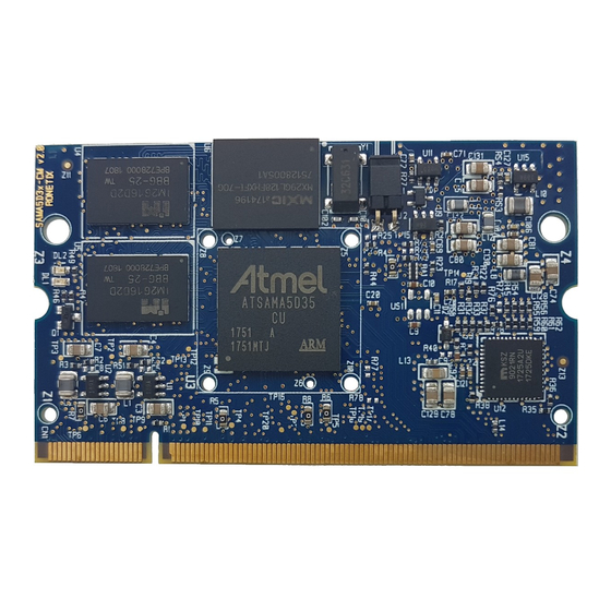
Section 5 Computer Module (CM) Board Overview The CM (CPU Module) board is the heart of the system. It connects to the Main Board through a SO- DIMM200 interface. It carries the SAMA5D3 series processor and external memories. The CM board s e r v e s m i n i m a l C P U... - Page 12 Figure 5-1. CM from EMBEST SAMA5D3x-EK User Guide 11180A–ATARM–30-Jan-13 Downloaded from Elcodis.com electronic components distributor...
- Page 13 Figure 5-2. CM from RONETIX SAMA5D3x-EK User Guide 11180A–ATARM–30-Jan-13 Downloaded from Elcodis.com electronic components distributor...
- Page 14 Figure 5-3. Board Architecture Nand Flash Nand Flash Nand Flash N N a a n n d d F F l l a a s s h h Nand Flash Nand Flash Nand Flash Nand Flash Nand Flash Nand Flash Nand Flash Nand Flash Nand Flash...
-
Page 15: Equipment List
Equipment List The CM board is built around a Cortex A5-based microcontroller (BGA 324 package) with external mem- ory and Gigabit Ethernet PHYsical Layer Transceiver. 5.2.1 Devices Table 5-2. CM Board Specifications Characteristic Specifications CPU Module (10 layers) Dimensions in mm: (L x W x H) 67.60 *(40 to 47) * 5 max Processor... -
Page 16: Boot Options
Functional Blocks 5.3.1 Processor The CM board is equipped with an Atmel ARM-based embedded MPU, as listed below, in a BGA324-ball BGA package. The four devices share an identical footprint. All four share the CM board PCB with minor configuration differences. -
Page 17: Clock Circuitry
hardware accelerated engines for encryption (AES, TDES) and hash function (SHA), the SAMA5D3 ensures anti-cloning, code protection and secure external data transfers. Please refer to Section 2.2 ”Evaluation Board Specifications” on page 2-3 for details. The processor runs at frequencies up to 536 MHz for the core and up to 166 MHz for the system bus. 5.3.2 Clock Circuitry The CM includes 3 clock sources:... - Page 18 Table 5-5. Supply Group Configuration Nominal Name Powers Component From Main 3.3V, SODIMM200 3.3V VDDANA the Analog to Digital Converter connector the core, including the processor, the 1.2V VDDCORE Regulator on-board embedded memories and the peripherals 1.2V VDDUTMIC The USB device and Host UTMI + core Regulator on-board 1.2V VDDPLLA...
- Page 19 Figure 5-5. RONETIX Power Supply Soft-Start Time EN Input High Threshold EN Input Low Threshold SEE TABLE 1 VDD_CORE LQM2HPN1R0MG0L 22u/6V3 22u/6V3 VOUT 0402 100k SC189ASKTRT 1V0 2k49/1% 10k/1% POWER_ENABLE SEE TABLE 1 GND pins are provided and should be VDDIODDR LQM2HPN1R0MG0L 22u/6V3...
- Page 20 Figure 5-6. RONETIX Power Supply (Continued) (3V3) VDD_IOM VDD_IOP0 VDD_IOP1 VDD_CORE U3-A 100n/10V 100n/10V VDDIOM VDDCORE 100n/10V 100n/10V VDDIOM VDDCORE 100n/10V VDDCORE 100n/10V GNDIOM VDDCORE 100n/10V GNDIOM VDDCORE 100n/10V VDDCORE 100n/10V 100n/10V VDDIOP0 VDDCORE 100n/10V VDDIOP0 100n/10V VDDIOP1 GNDCORE 100n/10V VDDIOP1 GNDCORE GNDCORE...
-
Page 21: Memory
5.3.5 Memory 5.3.5.1 Memory Organization The SAMA5D3 series processor features a DDR/SDR memory interface and an External Bus Interface (EBI) to permit interfacing to a wide range of external memories and to almost any kind of parallel peripheral. 5.3.5.2 Resources allocation. This section describes the memory devices that equip the SAMA5D3 series-CM board. - Page 22 Figure 5-8. RONETIX DDR2 Memory DDR_ADDR Address and control traces may not exceed 1.3 inches (33.0 mm). U3-H 12.09.2012 Address and control traces must be length-matched to within 0.1 inch (2.54 mm). DDR_A0 DDR_A[0-13] Chenged U4 and U5 Address and control traces must match the data group trace lengths to within 0.25 inches (6.35 mm). DDR_A0 DDR_A1 From MT47H64M16HR-25H to MT47H128M16RT-3:C...
- Page 23 Figure 5-9. EMBEST External Memory JS28F128P33TF70A JS28F128P33TF70A FLASH_A1 M_EBI_D0 FLASH_A2 M_EBI_D1 FLASH_A3 M_EBI_D2 FLASH_A4 M_EBI_D3 FLASH_A5 M_EBI_D4 FLASH_A6 M_EBI_D5 FLASH_A7 M_EBI_D6 FLASH_A8 M_EBI_D7 FLASH_A9 M_EBI_D8 FLASH_A10 M_EBI_D9 FLASH_A11 M_EBI_D10 DQ10 FLASH_A12 M_EBI_D11 DQ11 FLASH_A13 M_EBI_D12 DQ12 FLASH_A14 M_EBI_D13 DQ13 FLASH_A15 M_EBI_D14 DQ14 FLASH_A16...
-
Page 24: Serial Peripheral Interface Controller (Spi)
Figure 5-10. RONETIX External Memory U3-G PE0/A0(NBS0) A1_NOR PE1/A1 A2_NOR PE2/A2 A3_NOR VDD_IOM PE3/A3 A4_NOR PE4/A4 A5_NOR PE5/A5 A6_NOR PE6/A6 NOR FLASH A7_NOR PE7/A7 A8_NOR 100k PE8/A8 A9_NOR PE9/A9 A10_NOR PE26/NCS0/TXD2 PE10/A10 0402 A11_NOR NWE_NOR/NAND_WE PE11/A11 A12_NOR NRD_NOR/NAND_OE PE12/A12 A13_NOR NRST PE13/A13 2;7;8... -
Page 25: Serial Dataflash
Figure 5-11. EMBEST Serial DataFlash on SPI VDDIOP1 470K 470K MN10 MN10 AT25DF321A AT25DF321A VDDIOP1 PD11 (SPI0_MOSI) PD10 (SPI0_MIS0) PD12 (SPI0_SPCK) 100nF 100nF HOLD VDDIOP1 SERIAL DATAFLASH MN11 MN11 NL17SZ126 NL17SZ126 VDDIOP1 OE_Dataflash OE_Nandflash PD13 100nF 100nF BAT54C BAT54C BOOT_CS_OFF Figure 5-12. -
Page 26: 1-Wire Eeprom
5.3.7 1-Wire EEPROM The SAMA5D3 series-CM board uses 1-Wire device as "soft label" to store the information such as chip type, manufacture name, production date, etc. Only page 1 is used. Be careful not to modify the information contained in this page. Pages 2 to n remain free for the user. -
Page 27: Tri-Speed Ethernet Phy
5.3.8 Tri-Speed Ethernet PHY The SAMA5D3 series-CM board is equipped with a MICREL PHY devices (MICREL KSZ9021/31) oper- ating at 10/100/1000 Mbps. The board supports RGMII interface mode. The Ethernet interface consists of 4 pairs of low voltage differential pair signals designated from GRX± and GTx± plus control signals for link activity indicators. - Page 28 Figure 5-16. RONETIX GEthernet ETH0 ETH_DVDDL 2A ! max 345mA--> BLM21PG221SN1D C128 22u/6V3 22u/6V3 ETH_AVDDL 2A ! max 205mA--> BLM21PG221SN1D C129 ETH_AVDDH VDD_IOP1 22u/6V3 22u/6V3 max ?mA--> ETH_AVDDL_PLL 2A ! 0.5A ! max ?mA--> max 563mA--> ETH_V1 max 13mA--> BLM21PG221SN1D LQM2HPN1R0MG0L BLM15AG121SN1D C131...
-
Page 29: Indicators
5.3.9 Indicators There are two LEDs on the SAMA5D3 series-CM board that can be controlled by the user. The red LED provides an indication that power is supplied to the board and is controlled via software. The blue LED is controlled via GPIO pins. Figure 5-17. -
Page 30: Sodimm200 Interface
5.3.10 SODIMM200 Interface The SAMA5D3 series-CM board uses SODIMM200 card edge connector to interface with the MB board. Please refer to Figure 6-44 on page 6-44 5.3.11 Connectors The diagram below shows the mechanical dimensions of the SAMA5D3 series-CM Module outline and the mounting holes. -
Page 31: Embest Schematics
EMBEST Schematics This section contains the following schematics: Block Diagram SAMA5D3x Power SAMA5D3x NOR and NAND 4 Gb DDR2 SAMA5D3x Dataflash, 1-wire, LED Ethernet 200-pin SODIMM SAMA5D3x-EK User Guide 5-21 11180A–ATARM–30-Jan-13 Downloaded from Elcodis.com electronic components distributor... - Page 32 3V3 INPUT VBAT 128Mb ANALOG Reference FLASH ATMEL USB A,B,C SAMA5D3 SERIES DDR2 ARM CORTEX A5-BASED PROCESSOR SDRAM NAND FLASH PIO A,...E PIO A,...E PIO A&D PIO B&E SERIAL 10/100/1000 FAST ONE WIRE SERIAL DATA ETHERNET EEPROM EEPROM FLASH PIO C http://arm.embedinfo.com...
- Page 33 VCC_3V3 VDDIOP1 180ohm at 100MHz 180ohm at 100MHz VCC_1V2 MN15 MN15 RT9018B-18GSP RT9018B-18GSP VCC_3V3 NTRST 100nF 100nF 100nF 100nF 180ohm at 100MHz 180ohm at 100MHz VOUT C131 C131 C132 C132 C134 C134 100nF 100nF 10uF 10uF 10uF 10uF 23.7K 1% 23.7K 1% C0603 C0603...
- Page 34 MN2E MN2E M_EBI_A0 TP21 TP21 MN2F MN2F SAMA5D3x_BGA324 SAMA5D3x_BGA324 SAMA5D3x_BGA324 SAMA5D3x_BGA324 DDR_A[0..13] PE0_A0/NBS0 FLASH_A1 PE1_A1 DDR_A0 FLASH_A2 DDR_A0 PE2_A2 DDR_A1 FLASH_A3 DDR_A1 PE3_A3 DDR_A2 FLASH_A4 DDR_A2 PE4_A4 DDR_A3 FLASH_A5 DDR_A3 PE5_A5 DDR_A4 FLASH_A6 DDR_A4 PE6_A6 DDR_A5 FLASH_A7 DDR_A5 PE7_A7 DDR_A6 FLASH_A8 JS28F128P33TF70A JS28F128P33TF70A...
- Page 35 DDR_D[0..31] DDR_A[0..13] DDR_A0 DDR_D0 DDR_A0 DDR_D16 DDR_A1 DDR2 SDRAM DDR2 SDRAM DDR_D1 DDR_A1 DDR2 SDRAM DDR2 SDRAM DDR_D17 DDR_A2 DDR_D2 DDR_A2 DDR_D18 MT47H128M16RT MT47H128M16RT MT47H128M16RT MT47H128M16RT DDR_A3 DDR_D3 DDR_A3 DDR_D19 DDR_A4 DDR_D4 DDR_A4 DDR_D20 DDR_A5 DDR_D5 DDR_A5 DDR_D21 DDR_A6 DDR_D6 DDR_A6 DDR_D22 DDR_A7...
- Page 36 VDDIOP1 470K 470K MN10 MN10 AT25DF321A AT25DF321A VDDIOP1 PA[0..31] {7} PC[0..31] {7} MN2A MN2A MN2C MN2C PD11 (SPI0_MOSI) SAMA5D3x_BGA324 SAMA5D3x_BGA324 SAMA5D3x_BGA324 SAMA5D3x_BGA324 PD10 (SPI0_MIS0) PD12 (SPI0_SPCK) PA0_LCDDAT0 PC0_ETX0 100nF 100nF PA1_LCDDAT1 PC1_ETX1 HOLD PA2_LCDDAT2 PC2_ERX0 PA3_LCDDAT3 PC3_ERX1 PA4_LCDDAT4 PC4_ETXEN PA5_LCDDAT5 PC5_ECRSDV PA6_LCDDAT6 PC6_ERXER...
- Page 37 AVDDL_PLL NRST {2,3,7} 10nF 10nF 10nF 10nF 10uF 10uF 4.7K 4.7K VDDIOP1 PB[0..31] {5,7} G125CK PB18 INT_GETHR PB25 VDDIOP1 180ohm at 100MHz 180ohm at 100MHz AVDDH GMDIO PB17 VDDIOP1 10nF 10nF 10nF 10nF 10nF 10nF 10uF 10uF 4.99K 1% 4.99K 1% C100 C100 C101...
- Page 38 VCC_5V VCC_5V VCC_5V_1 VCC_5V_2 VDDBU VCC_5V_3 VCC_5V_4 GND1 VBAT PE23 PE29 PA[0..31] PE23 PE29 PE24 PE30 C122 C122 PE24 PE30 PE25 PE31 PE25 PE31 PE26 VDDIOM PE26 GND2 VDDIOM VDDIOM_1 VDDIOM_2 PC25 PC24 PC25 PC24 PC23 PC22 C123 C123 PC23 PC22 PC21 PC20...
-
Page 39: Ronetix Schematics
RONETIX Schematics This section contains the following schematics: Main Sheet SODIMM 200 Power Supply CPU Power Supply DDR2 interface FI: NAND, NOR, Serial, I2C, 1-wire Ethernet USB, JTAG, LEDs Bus Interface 5-22 SAMA5D3x-EK User Guide 11180A–ATARM–30-Jan-13 Downloaded from Elcodis.com electronic components distributor... - Page 40 SCHEMATICS: SAMA5D3x-CM SHEET # SHEET NAME DATE: DESCRIPTION REVISION STATUS MAIN SAMA5D3x-CM v2.0 15.03.2012 OPEN SODIM200 SAMA5D3x-CM v2.0 20.09.2012 CLOSE POWER SUPPLY Changes Rev2.0 CPU-POWER SUPPLY 1. SoDIMM200 change: * PB13 pin 144 with 0R DNP * PB12 pin 146 with 0R populated DDR2 INTERFACE 2.
- Page 41 Power Supply 2.5V SODIM200_PCB_PADS VCC 5V Vbat VCC 5V VCC 5V VCC 5V PE23/A23_NOR/CTS2 PE29/NWR1(NBS1)/TCLK2 PE24/RTS2 PE30/NWAIT PE25/RXD2/1-Wire PE31/IRQ/PWML1 PE26/NCS0/TXD2 VDD_IOM VDD_IOM PC25/SPI1_NPCS0 PC24/SPI1_SPCK PC23/SPI1_MOSI PC22/SPI1_MISO PC21/RD0 PC20/RF0 PC19/RK0 PC18/TD0 PC17/TF0 PC16/TK0 PC9/EMDIO PC8/EMDC/TCLK5 PC7/EREFCK/TIOB5 PC6/ERXER/TIOA5 PC4/ETXEN/TIOB4 PC5/ECRSDV/TCLK4 PC2/ERX0/TCLK3 PC3/ERX1/TIOA4 PC0/ETX0/TIOA3 PC1/ETX1/TIOB3 POWER_ENABLE...
- Page 42 Soft-Start Time EN Input High Threshold EN Input Low Threshold SEE TABLE 1 RS1=(Vout-1)xRS2 TABLE 1 VDD_CORE VDD_CORE 1.0V 1.2V 1.25V 0R (JUMP) 2kOhm 1% 2k5ohm 1% 2k49ohm 1% LQM2HPN1R0MG0L 10kOhm 1% 10kOhm 1% 22u/6V3 BU10TD3WG-TR BU12TD3WG-TR 22u/6V3 VOUT 0402 100k SC189ASKTRT 1V0 2k49/1%...
- Page 43 ADVREF TP10ADVREF TP11GND (3V3) VDD_IOM VDD_IOP0 VDD_IOP1 VDD_CORE U3-A 100n/10V 100n/10V VDDIOM VDDCORE 100n/10V 100n/10V VDDIOM VDDCORE 100n/10V VDDCORE 100n/10V GNDIOM VDDCORE 100n/10V GNDIOM VDDCORE 100n/10V VDDCORE 100n/10V 100n/10V VDDIOP0 VDDCORE 100n/10V VDDIOP0 100n/10V VDDIOP1 GNDCORE 100n/10V VDDIOP1 GNDCORE GNDCORE GNDIOP GNDCORE GNDIOP...
- Page 44 DDR_ADDR Address and control traces may not exceed 1.3 inches (33.0 mm). U3-H 12.09.2012 Address and control traces must be length-matched to within 0.1 inch (2.54 mm). DDR_A0 DDR_A[0-13] Chenged U4 and U5 Address and control traces must match the data group trace lengths to within 0.25 inches (6.35 mm). DDR_A0 DDR_A1 From MT47H64M16HR-25H to MT47H128M16RT-3:C...
- Page 45 U3-G PE0/A0(NBS0) A1_NOR PE1/A1 A2_NOR PE2/A2 A3_NOR VDD_IOM PE3/A3 A4_NOR PE4/A4 A5_NOR VDD_IOM PE5/A5 A6_NOR PE6/A6 NOR FLASH A7_NOR NAND FLASH PE7/A7 L3 & L8 A8_NOR 100k PE8/A8 Zo=60 ohms +/-10% L3 & L8 A9_NOR PE9/A9 100k Zo=60 ohms +/-10% A10_NOR PE26/NCS0/TXD2 PE10/A10...
- Page 46 ETH_DVDDL 2A ! max 345mA--> BLM21PG221SN1D C128 22u/6V3 22u/6V3 ETH_AVDDL 2A ! max 205mA--> BLM21PG221SN1D C129 ETH_AVDDH VDD_IOP1 22u/6V3 22u/6V3 max ?mA--> ETH_AVDDL_PLL 2A ! 0.5A ! max ?mA--> max 563mA--> ETH_V1 max 13mA--> BLM21PG221SN1D LQM2HPN1R0MG0L BLM15AG121SN1D C131 C130 C106 C107 22u/6V3 22u/6V3...
- Page 47 SOFT MODEM Cl=Cs+[C1xC2]/[C1+C2] if C1=C2 => C100 C1,2=2[Cl-Cs] !!! U3-B Cl is load capacitance of the cristal 27p/50V top/bot CS is the stray capacitance on the printed circuit board, typically a value of 5pf can be used for calculation top/bot CPX32-12.000MHz XOUT C101...
- Page 48 U3-C SAMA5D3x PA0/LCDDAT0 PA0/LCDDAT0 PA1/LCDDAT1 PA1/LCDDAT1 PA2/LCDDAT2 PA2/LCDDAT2 PA3/LCDDAT3 PA3/LCDDAT3 PA4/LCDDAT4 PA4/LCDDAT4 PA5/LCDDAT5 PA5/LCDDAT5 PA6/LCDDAT6 PA6/LCDDAT6 PA7/LCDDAT7 PA7/LCDDAT7 PA8/LCDDAT8 PA8/LCDDAT8 PA9/LCDDAT9 PA9/LCDDAT9 PA10/LCDDAT10 PA10/LCDDAT10 PA11/LCDDAT11 PA11/LCDDAT11 PA12/LCDDAT12 PA12/LCDDAT12 PA13/LCDDAT13 PA13/LCDDAT13 PA14/LCDDAT14 PA14/LCDDAT14 PA15/LCDDAT15 PA15/LCDDAT15 PA16/LCDDAT16/ISI_D0 PA16/LCDDAT16/ISI_D0 PA17/LCDDAT17/ISI_D1 PA17/LCDDAT17/ISI_D1 PA18/LCDDAT18/TWD2/ISI_D2 PA18/LCDDAT18/TWD2/ISI_D2 PA19/LCDDAT19/TWCK2/ISI_D3 PA19/LCDDAT19/TWCK2/ISI_D3 PA20/LCDDAT20/PWMH0...
-
Page 49: Main Board (Mb)
Section 6 Main Board (MB) Main Board Overview The SAMA5D3 series-MB board serves as the main board that carries the CPU module. It features all necessary peripheral devices and interfaces for processor evaluation. Figure 6-1. Main Board Top View SAMA5D3x-EK User Guide 11180A–ATARM–30-Jan-13 Downloaded from Elcodis.com... - Page 50 Figure 6-2. MB Board Layout Commented SAMA5D3x-EK User Guide 11180A–ATARM–30-Jan-13 Downloaded from Elcodis.com electronic components distributor...
-
Page 51: Equipment List
6.1.1 Equipment List The SAMA5D3 series-MB is a full featured mother board . Due to the embedded module concept this baseboard can be used with every available SAMA5D3 series-CM CPU module. 6.1.2 Technical specifications Table 6-1. MB Technical Specifications Characteristic Specifications Supported Module All SAMA5D3 series computer modules... - Page 52 6.1.3 Devices List of the MB board peripherals: Two EMAC PHY One audio CODEC Two high speed MCI card interfaces Two CAN transceivers One RS232 port with level translator features USART1 One smart DAA port Two USB host port One USB host/device port On-board power regulation LCD/ISI extension interface HDMI interface...
-
Page 53: Function Blocks
Figure 6-3. MB Architecture COM1 or COM1 or On Board JTAG On Board JTAG VCC 5V Jack VCC 5V Jack Audio Audio Audio Audio MIC1 MIC1 MCI0 MCI0 CAN0 & 1 CAN0 & 1 DBGU DBGU Bridge Bridge ZIGBEE ZIGBEE Modem Modem RS232... - Page 54 Figure 6-4. SODIMM Interface on MB VDDIOP0 JP9 for BMS Config: When Open,BMS=1: Boot on embeded ROM When Close,BMS=0: Boot on External memory 4.7k 4.7k VCC5V_1 VCC5V_2 VCC5V_3 VCC5V_4 GND1 VBAT VBAT 4,12 PE23 PE29 Z B _ R S T N PE29 6,13 PE23...
- Page 55 6.2.2 Power Supplies The SAMA5D3 series-MB board is supplied with a simple external 5 VCC power supply. The SAMA5D3 series-MB Board features one adjustable LDO. It accepts DC in 5V power and outputs a regulated +3.3V to most other circuits on the board through four 3.3V rails. 6.2.2.1 Supply Group Configuration This LDO is enabled through a dual FET scheme.
-
Page 56: Debug Jtag/Ice And Dbgu
6.2.3 Debug JTAG/ICE and DBGU The Main Board embeds a SEGGER J-Link-on-Board based on an ATSAM3U4C LQFP100. This processor provides the functions of JTAG and bridge USB/Serial DBGU port. The J-Link-OB-ATSAM3U4C was designed in order to provide a low-cost, space-saving and onboard alternative to the general J-Link. -
Page 57: Usart
6.2.3.1 Disabling J-Link-OB-SAM3U128 The J-Link-OB-ATSAM3U4C may be disabled by Jumper JP15 (PA26, pin 25 of the ATSAM3U4C CPU). Jumper not fitted: J-Link-OB-ATSAM3U4C is enabled and fully functional Jumper fitted: J-Link-OB-ATSAM3U4C is disabled The pin uses internal pull-up (so if JP15 is not required, simply leave the pin on the J-Link-OB- ATSAM3U4C open), jumper shortens to ground. -
Page 58: Usb Ports
6.2.5 USB Ports The SAMA5D3 series-MB features three USB communication ports: Port A Host High Speed (EHCI) and Full Speed (OHCI) multiplexed with USB Device High Speed Micro AB connector, J20 Port B Host High Speed (EHCI) and Full Speed (OHCI) standard type A connector, J19 upper port Port C Host Full Speed (OHCI) only... -
Page 59: Ethernet 10/100 (Emac) Port
Figure 6-9. USB Ports B and C USBB_DP 3 USBB_DM 3 MN19 MN19 MN14 MN14 EN5V_HDB OUTA PD26 C102 C102 220ohm at 100MHz 220ohm at 100MHz OVCUR_USB PD28 PD28 FLGA 100n 100n C103 C103 C101 C101 100n 100n PD27 FLGB V C C V C C G N D... - Page 60 Figure 6-10. ETH0 Port ETH0 10Base-T/100Base-TX/1000BASE-T T R D 4 + T R D 4 + T 4 / A T 4 / A T 4 / B T 4 / B T R P 4 + T R P 4 + ETH0_RX2+ C125 100n C125 100n...
-
Page 61: Audio
6.2.7 Audio The Main Board includes a WM8904 CODEC for digital sound input and output. This interface includes audio jacks for micro input (J13) and headphone line output (J15). This interface can be used to play and record audio. The WM8904 has left and right channel line inputs, a microphone input and an on-board microphone, a left and right headphone output. -
Page 62: Hdmi Transmitter Interface
6.2.8 HDMI Transmitter Interface The Main Board (MB) is equipped with an HDMI transmitter interface. The SiI9022/9024 HDMI Tx provides a complete solution for transmitting HDMI compliant digital audio/video. Specialized audio/video processing is available within the transmitter to easily and cost- effectively add HDMI capability to consumer electronics devices. -
Page 63: Wire Eeprom
6.2.9 1-Wire EEPROM The Main Board (MB) also features a 1-Wire device as "software identification label" to store information such as chip type, manufacture name, production date, etc. Figure 6-14. 1-Wire on MB ONE WIRE EEPROM R144 R144 1.5k 1.5k MN16 MN16 N E _ W I R E... -
Page 64: Smart Daa
6.2.11 Smart DAA The SAMA5D3 series-MB features a smart DAA chip to drive an analog telephone line on RJ11 6P4C port (J16). Figure 6-16. Smart DAA 220ohm at 100MHz 220ohm at 100MHz 6.81M 6.81M MN11 MN11 MMBD3004S-7-F MMBD3004S-7-F TEST 470p 470p RJ11 MMBD3004S-7-F... -
Page 65: Sd/Mmc Interface
6.2.12 SD/MMC Interface SD/MMC is a standard Secure Digital / MultiMedia Card interface. The Main Board (MB) has two high-speed Multimedia Card Interfaces (MCI). The first interface is used as a 8-bit interface (MCI0), connected to a SD/MMC card slot. The second interface is used as a 4-bit interface (MCI1), connected to a MicroSD card slot. -
Page 66: Zigbee
One Wake up, push button to bring the processor out of low power mode (BP2) One User momentary Push Button One Disable CS Push Button 6.2.15.1 Reset When pressed and released, causes a power-on reset of the SAMA5D3 series-EK (boards MB, CM and DM). 6-18 SAMA5D3x-EK User Guide 11180A–ATARM–30-Jan-13... -
Page 67: Analog Reference
6.2.15.2 CS_BOOT Button The CS_BOOT can be used to prevent the system to boot out of external memories (NandFlash, SPI flash). The purpose is mainly to execute the SAM-BA part of the ROM code. 2 methods can be used: 1. Press the CS_BOOT and power-cycle the board. 2. -
Page 68: Expansion Ports
Figure 6-20. Analog Reference VDDANA ANALOG Reference 3V R143 R143 JP14 JP14 1.5k 1.5k ADVREF C112 C112 100n 100n C113 C113 2.2u 2.2u LM4040BIM3-3.0+T LM4040BIM3-3.0+T 6.2.17 Expansion Ports Three 40-pin headers (J1, J2, J3) are provided on the board to allow for the PIO connection of various expansion cards that could be developed by the users or other sources. - Page 69 Figure 6-22. LCD Expansion R147 R147 R148 R148 Z B _ I R Q 0 Z B _ I R Q 1 PE30 10,3,6 PE31 R146 R146 R149 R149 T W C K 1 ( S P I 1 _ N P C S 2 ) T W D 1 ( S P I 1 _ N P C S 1 ) 13,3 PC26...
-
Page 70: Configuration
Configuration This section describes the PIO usage, the jumpers, the test points and the solder drops of a SAMA5D3 series-EK board. Table 6-2. Jumpers and Solderdrops Reference Default Function VDDIOP0 or 5V selection for J1 VDDIOP0 or 5V selection for J2 VDDIOP0 or 5V selection for J3 CLOSE Backup supply on/off... -
Page 71: Pio Usage And Interface Connectors Details
Table 6-3. Default Not Populated Parts Page Reference Function L38,L39,L40,L41 Optional HDMI EMI filter HDMI chip I2C address setting R266 Optional for I2S PCLK Optional for LCD PCLK R162,R170,R171,R172,R176,R177,C122,C123 Optional for KSZ8041NL R144 Optional pull up for DS28EC20P R127 Optional for ADC trigger R79,R106,R107,R109,R113,R110,R112,R111,J9 Optional JTAG SAM3U JTAG selection... -
Page 72: Jtag/Ice Connector
6.4.2 JTAG/ICE Connector Figure 6-25. JTAG J9 Table 6-5. JTAG/ICE Connector J9 Signal Descriptions Mnemonic Signal Description This is the target reference voltage. It is used to check if the target has power, to create the logic-level reference for the 3.3V power input comparators, and to control the output logic levels to the target. -
Page 73: Usb Type A Dual Port
Table 6-5. JTAG/ICE Connector J9 Signal Descriptions Mnemonic Signal Description TDO JTAG Test Data Output JTAG data output from target CPU. Typically connected to - Serial data input from the TDO on target CPU. target. Common ground nSRST RESET Active-low reset signal. Target CPU reset signal. Common ground This pin is not connected in SAM-ICE. -
Page 74: Usb Microab
Table 6-6. USB Type A Dual Port J19 Signal Descriptions Mnemonic Signal Description Vbus - USB_A 5V power DM - USB_A Data minus DP - USB_A Data plus Common ground Vbus - USB_A 5V power DM - USB_A Data minus DP - USB_A Data plus Common ground... -
Page 75: Jtag Ob Usb Microab
6.4.5 JTAG OB USB MicroAB Figure 6-28. USB JTAG OB MicroAB connector J14 Table 6-8. USB JTAG OB MicroAB connector J14 Signal Descriptions Mnemonic Signal description Vbus 5V power Data minus Data plus On the Go Identification Common ground 6.4.6 HDMI Connector Figure 6-29. -
Page 76: Rs232 Connector With Rts/Cts Handshake Support
Table 6-9. HDMI Type A Female Connector J25 Pin Num TMDS Data 2+ TMDS Data 2 Shield TMDS Data 2- TMDS Data 1+ TMDS Data 1 Shield TMDS Data 1- TMDS Data 0+ TMDS Data 0 Shield TMDS Data 0- TMDS Clock + TMDS Clock Shield TMDS Clock -... -
Page 77: Daa Rj11 Socket (6P4C)
6.4.8 DAA RJ11 Socket (6P4C) Figure 6-31. DAA RJ11 Socket J16 Table 6-11. DAA RJ11 Socket J16 Signal Descriptions Mnemonic Signal Description 1, 2, 5, 6 No connection RING side of ordinary telephone line TIP side of ordinary telephone line 6.4.9 CAN RJ12 Socket (6P6C) Figure 6-32. -
Page 78: Sd/Mmc Plus Mci0
6.4.10 SD/MMC Plus MCI0 Figure 6-33. SD Socket J7 Table 6-13. MicroSD Socket J7 Signal Descriptions Mnemonic Signal Description DAT3 Data bit Command line Command line Supply voltage 3.3V Clock / command line PD17 Card detect DAT0 Data bit DAT1 Data bit DAT2 Data bit... -
Page 79: Microsd Mci1
6.4.11 MicroSD MCI1 Figure 6-34. MicroSD Socket J6 Table 6-14. MicroSD Socket J6 Signal Descriptions Mnemonic Signal Description DAT2 PB22 Data bit 2 CD/DAT3 PB23 Card detect / data bit 3 PB19 Command line Supply voltage 3.3V PB24 Clock / command line Common ground DAT0 PB20... -
Page 80: Gigabit Ethernet Eth0 Rj45 Socket J17
6.4.12 Gigabit Ethernet ETH0 RJ45 Socket J17 Figure 6-35. Gigabit Ethernet RJ45 Socket J17 6.4.13 Ethernet ETH1 RJ45 Socket J24 Figure 6-36. Ethernet RJ45 Socket J24 6.4.14 ZigBee Socket J10 Figure 6-37. ZigBee Socket J10 Table 6-15. ZigBee Socket J10 Signal Descriptions Function Port Port... -
Page 81: Lcd Socket J21
6.4.15 LCD Socket J21 Figure 6-38. LCD Socket J21 Table 6-16. LCD Socket J21 HE10 Female LCD 2*15p Pin Num VDD3V3 VDD3V3 ZB_IRQ0 ZB_IRQ1 TWCK1 TWD1 LCDDAT15 LCDDAT13 LCDDAT14 LCDDAT12 LCDDAT0 LCDDAT1 LCDDAT2 LCDDAT3 LCDDAT4 LCDDAT5 LCDDAT6 LCDDAT7 LCDDAT8 LCDDAT9 LCDDAT10 LCDDAT11 SAMA5D3x-EK User Guide... -
Page 82: Lcd/Tsc Socket J22
6.4.16 LCD/TSC Socket J22 Figure 6-39. LCD/TSC Socket J22 Table 6-17. LCD/TSC Socket J22 HE10 Female LCD/TSC/QT 2*20p Pin Num 5V_LCD 5V_LCD LCDDAT16 LCDDAT17 LCDDAT18 LCDDAT19 LCDDAT20 LCDDAT21 LCDDAT22 LCDDAT23 LCDDISP LCDPWM LCDCSYNC LCDHSYNC LCDDEN LCDPCK AD0_XP AD1_XM AD2_YP AD3_YM AD4_LR ONE_WIRE GND1... -
Page 83: Isi Socket J11
6.4.17 ISI Socket J11 Figure 6-40. ISI Socket J11 Table 6-18. ISI Socket J11 HE10 Female ISI 2*15p Pin Num VDDISI VDDISI ZB_SLPTR ZB_RST TWCK1 TWD1 ISI_MCK ISI_VSYNC ISDI_HSYNC ISI_PCK ISI_D0 ISI_D1 ISI_D2 ISI_D3 ISI_D4 ISI_D5 ISI_D6 ISI_D7 ISI_D8 ISI_D9 ISI_D10 ISI_D11 SAMA5D3x-EK User Guide... -
Page 84: Isi_D1
6.4.18 PIO Usage Table 6-19. PIO A Pin Assignment and Signal Description Power Rail Signal Signal Signal Signal SAMA5-CM SAMA5-MB VDDIOP0 LCDDAT0 LCDDAT0 VDDIOP0 LCDDAT1 LCDDAT1 VDDIOP0 LCDDAT2 LCDDAT2 VDDIOP0 LCDDAT3 LCDDAT3 VDDIOP0 LCDDAT4 LCDDAT4 VDDIOP0 LCDDAT5 LCDDAT5 VDDIOP0 LCDDAT6 LCDDAT6 VDDIOP0 LCDDAT7... - Page 85 Table 6-20. PIO B Pin Assignment and Signal Description Power Rail Signal Signal Signal Signal SAMA5-CM SAMA5-MB VDDIOP1 GTX0 PWMH0 GETH CM VDDIOP1 GTX1 PWML0 GETH CM VDDIOP1 GTX2 GETH CM VDDIOP1 GTX3 GETH CM VDDIOP1 GRX0 PWMH1 GETH CM VDDIOP1 GRX1 PWML1...
-
Page 86: Isi_D9
Table 6-21. PIO C Pin Assignment and Signal Description Power Rail Signal Signal Signal Signal SAMA5-MB VDDIOP0 ETX0 TIOA3 ETX0 VDDIOP0 ETX1 TIOB3 ETX1 VDDIOP0 ERX0 TCLK3 ERX0 VDDIOP0 ERX1 TIOA4 ERX1 VDDIOP0 ETXEN TIOB4 ETXEN VDDIOP0 ECRSDV TCLK4 ECRSDV VDDIOP0 ERXER TIOA5... - Page 87 Table 6-22. PIO D Pin Assignment and Signal Description Power Rail Signal Signal Signal Signal SAMA5-MB VDDIOP1 MCI0_CDA MCI0_CDA VDDIOP1 MCI0_DA0 MCI0_DA0 VDDIOP1 MCI0_DA1 MCI0_DA1 VDDIOP1 MCI0_DA2 MCI0_DA2 VDDIOP1 MCI0_DA3 MCI0_DA3 VDDIOP1 MCI0_DA4 TIOA0 PWMH2 MCI0_DA4 VDDIOP1 MCI0_DA5 TIOB0 PWML2 MCI0_DA5 VDDIOP1 MCI0_DA6...
- Page 88 Table 6-23. PIO E Pin Assignment and Signal Description Power Rail Signal Signal Signal SAMA5-CM SAMA5-MB VDDIOM A0/NBS0 VDDIOM VDDIOM VDDIOM VDDIOM VDDIOM VDDIOM VDDIOM VDDIOM VDDIOM VDDIOM PE10 VDDIOM PE11 VDDIOM PE12 VDDIOM PE13 VDDIOM PE14 VDDIOM PE15 SCK3 VDDIOM PE16 CTS3...
-
Page 89: Io Expansion Port J1
6.4.19 IO Expansion Port J1 Figure 6-41. IO Expansion Socket J1 Table 6-24. IO Expansion Socket J1 HE10 Male 2*20 Signal Descriptions Signal Pin Num Signal VDDIOP0 / 5V VDDIOP0 / 5V PA16 PA17 PA18 PA19 PA20 PA21 PA22 PA23 PA24 PA25 PA10... -
Page 90: Io Expansion Port J2
6.4.20 IO Expansion Port J2 Figure 6-42. IO Expansion Socket J2 Table 6-25. Expansion Socket J2 HE10 Male 2*20 Signal Descriptions Signal Pin Num Signal VDDIOP0 / 5V VDDIOP0 / 5V PC16 PC17 PC18 PC19 PC20 PC21 PC22 PC23 PC24 PC25 PC10 PC26... -
Page 91: Io Expansion Port J3
6.4.21 IO Expansion Port J3 Figure 6-43. IO Expansion Socket J3 Table 6-26. Expansion Socket J3 HE10 Male 2*20 Signal Descriptions Signal Pin Num Signal VDDIOP0 / 5V VDDIOP0 / 5V PB10 PB31 PB12 PE23 PB14 PE24 PB15 PE25 PB19 PE26 PB20 PE29... -
Page 92: Sodimm Card Edge Socket
6.4.22 SODIMM Card Edge Socket The SAMA5D3 series-EK implements a SODIMM200 standard connector for CM board interfacing. Please note this is not an industry standard pin-out and that it is unlikely to be compatible with off the self SODIMM. Figure 6-44. SODIMM200 Socket CON1... - Page 93 Table 6-27. SODIMM200 CON1 Signal Descriptions PIOC PIOB PIOA SODIMM 200 PIOA PIOB PIOC Front Side Back Side VCC 5V VCC 5V VCC 5V VCC 5V VBAT CTS2 PE23 PE29 NWR1/NBS1 TCLK2 RTS2 PE24 PE30 NWAIT RXD2 PE25 PE31 PWML1 TXD2 PE26 VDDIOM...
-
Page 94: Isi_D2
Table 6-27. SODIMM200 CON1 Signal Descriptions PIOC PIOB PIOA SODIMM 200 PIOA PIOB PIOC LCDDAT4 LCDDAT5 LCDDAT6 LCDDAT7 LCDDAT8 LCDDAT9 PA10 LCDDAT10 LCDDAT11 PA11 LCDDAT12 PA12 PA13 LCDDAT13 LCDDAT14 PA14 PA15 LCDDAT15 ISI_D0 LCDDAT16 PA16 PA17 LCDDAT17 ISI_D1 ISI_D2 TWD2 LCDDAT18 PA18 PA19... - Page 95 Table 6-27. SODIMM200 CON1 Signal Descriptions PIOC PIOB PIOA SODIMM 200 PIOA PIOB PIOC GTX4 MCI1_CDA PB19 PB20 MCI1_DA0 GTX5 GTX6 MCI1_DA1 PB21 PB22 MCI1_DA2 GTX7 GRX4 MCI1_DA3 PB23 GRX5 MCI1_CK PB24 PB25 SCK1 GRX6 PB27 RTS1 PWMH1 USB A USBA_DP PB29 TXD1...
-
Page 96: Schematics
Schematics This section contains the following schematics: Block Diagram Describe SODIMM Power Supply HSMCI CAN & ZigBee & USART1 Audio Smart DAA HDMI USB Interface Miscellaneous LCD & ISI Segger - SAM3U 6-48 SAMA5D3x-EK User Guide 11180A–ATARM–30-Jan-13 Downloaded from Elcodis.com electronic components distributor... - Page 97 Sheet 4 POWER SUPPLY Sheet 4 Sheet 12 ANALOG Battery 3V3 INPUT RJ11 USBA USBB USBC VBAT SmartDAA HOST & DEVICE HOST HOST Sheet 8 ANALOG Reference 3V Sheet 11 USB A,B,C SmartDAA SAM3U DBGU USER INTERFACE ONE WIRE EEPROM Sheet 14 HE 14 HE 14...
- Page 98 REVISION HISTORY SAMA5D3x config SCHEMATICS CONVENTIONS DATA NOTE SAMA5D31 SAMA5D33 SAMA5D34 SAMA5D35 (1) Resistance Unit: "K" is "Kohm", "R" is "Ohm 2011.11 ORIGINAL RELEASED CAN0 CAN1 (2) "DNP" means the component is not populated 2012.03 SECOND RELEASED by default GMAC 2012.10 THIRD RELEASED EMAC...
- Page 99 VDDIOP0 VDDIOP0 JP9 for BMS Config: When Open,BMS=1: Boot on embeded ROM When Close,BMS=0: Boot on External memory 4.7k 4.7k VCC5V_1 VCC5V_2 SIP2 SIP2 VCC5V_3 VCC5V_4 MD2X20-H MD2X20-H 12,4 GND1 VBAT VBAT PE23 PE29 ZB_RSTN PE29 13,6 PE23 PE29 ISI_RST PE24 PE30 ZB_IRQ1...
- Page 100 ZEN056V230A16LS ZEN056V230A16LS BNX002-01 BNX002-01 BAT54CLT1G BAT54CLT1G VBAT 12,3 5V_INPUT J5 J5 SIP2 SIP2 100n 100n DC POWER JACK DC POWER JACK 100n 100n 5V/2A Input 100n 100n VOUT = 0.8V x (Rtop + Rbottom)/Rbottom PWR_EN 220ohm at 100MHz 220ohm at 100MHz PWR_EN IRLML2402 IRLML2402...
- Page 101 VDD_MCI0 VDD_MCI0 VDDIOP1 MCI0 SIP2 SIP2 100n 100n (MCI0_WP) (MCI0_CD) PD17 VDDIOP1 (MCI0_DA1) (MCI0_DA0) (MCI0_CK) (MCI0_CDA) (MCI0_DA3) (MCI0_DA2) PB10 7SDMM-B0-2211 7SDMM-B0-2211 RR42 RR42 VDD_MCI0 (MCI0_DA4) (MCI0_DA5) IRLML6402 IRLML6402 4.7k 4.7k (MCI0_DA6) (MCI0_DA7) RR4,RR5,RR42 near SODIMM place SD/MMCPlus CARD INTERFACE - MCI0 VDDIOP1 VDD_MCI1 MCI1...
- Page 102 CAN INTERFACE SIP2 SIP2 120R 120R CANH CANTX0 CAN0 PD15 CANL VDDIOP0 VDDIOP1 CANRX0 MJM0606GE06-H MJM0606GE06-H PD14 SN65HVD234DR SN65HVD234DR 100n 100n SIP2 SIP2 120R 120R CAN1 CANH CANTX1 13,3 PB15 CANL VDDIOP0 VDDIOP1 CANRX1 MJM0606GE06-H MJM0606GE06-H 13,3 PB14 SN65HVD234DR SN65HVD234DR 100n 100n VDDIOP1...
- Page 103 220ohm at 100MHz 220ohm at 100MHz C140 C140 C141 C141 C137 C137 C142 C142 100n 100n 4.7u 4.7u 100n 100n AUDIO_GND AUD_1V8 AVDD1V8 AVDD1V8 220ohm at 100MHz 220ohm at 100MHz 2.2u 2.2u AUDIO_GND VDDIOP0 AUD_1V8 C138 C138 C139 C139 100n 100n HEADPHONE R122...
- Page 104 220ohm at 100MHz 220ohm at 100MHz 0805 6.81M 6.81M MN11 MN11 MMBD3004S-7-F MMBD3004S-7-F TEST 470p 470p RJ11 D5 MMBD3004S-7-F MMBD3004S-7-F DAA_GND 220ohm at 100MHz 220ohm at 100MHz TB3100M-13-F TB3100M-13-F 470p 470p MJM0606GE06-H MJM0606GE06-H 0805 6.81M 6.81M AVDD 100n 100n 100n 100n 100n 100n...
- Page 105 HDMI Spec. +4.8V < PVDD5 < +5.3V HDMI_INT 13,3 PC29 PVDD5 1812L160/12 1812L160/12 RB160M-60 RB160M-60 Type A connector TWD0 R272 R272 13,3,7 PA30 TWCK0 R273 R273 R105 R105 R104 R104 100n 100n 13,3,7 PA31 4.7k 4.7k 4.7k 4.7k LOW:72h(Defult) HPD_SiI R108 R108 4.7k...
- Page 106 ETH1 VDDIOP0 C122 C122 100n 100n 10Base-T/100Base-TX GND_ETH1 C100 C100 220ohm at 100MHz 220ohm at 100MHz R136 R136 R170 R170 R162 R162 49.9R 49.9R 49.9R 49.9R EARTH_ETH1 EARTH_ETH1 GND_ETH1 RR17 RR17 MN20 MN20 REF_CLK/B-CAST_OFF E1_TXCK E1_TX1 TXD1 E1_TX0 R176 R176 TXD0 E1_TXEN TXEN...
- Page 107 USB HOST B&C INTERFACE USBB_DP 3 USBB_DM 3 MN19 MN19 MN14 MN14 EN5V_HDB OUTA PD26 C102 C102 220ohm at 100MHz 220ohm at 100MHz OVCUR_USB PD28 PD28 FLGA 100n 100n C103 C103 C101 C101 100n 100n PD27 FLGB EN5V_HDC OUTB SN74LVC2GU04 SN74LVC2GU04 C105 C105...
- Page 108 PUSH BUTTON ANALOG Reference 3V VBAT VDDANA R141 R141 R142 R142 100k 100k 1.5k 1.5k R143 R143 JP14 JP14 NRST 1.5k 1.5k NRST 10,14,3 ADVREF WAKE UP C112 C112 WAKE UP 100n 100n C113 C113 PB_USER1 PB_USER1 2.2u 2.2u LM4040BIM3-3.0+T LM4040BIM3-3.0+T PE27 13,3,9...
- Page 109 ZB_IRQ0 ZB_IRQ1 R147 R147 R148 R148 PE31 PE30 10,3,6 R146 R146 TWCK1(SPI1_NPCS2) TWD1(SPI1_NPCS1) R149 R149 13,3 PC26 13,3 PC27 LCDDAT15 PA15 LCDDAT13 RR13 RR13 PA13 LCDDAT14 PA14 LCDDAT12 PA12 LCDDAT0 LCDDAT1 LCDDAT2 RR12 RR12 LCDDAT3 LCDDAT4 RR11 RR11 LCDDAT5 LCDDAT6 LCDDAT7 LCDDAT8 RR43C...
- Page 110 VCC_3V3_DEBUG VCC_3V3_DEBUG MN17 MN17 NRST_3U RESET TMS_3U TDI_3U TDI_3U GND1 TDO_3U TRSTIN TCK_3U R131 R131 TDO/TRACESWO PA0/PGMNCMD TCK_3U TRSTOUT TDO_3U TCK/SWCLK PA1/PGMRDY GND2 TMS_3U TMS/SWDIO PA2/PGMNOE TRESIN TC2050-IDC TC2050-IDC PA3/PGMNVALID ERASE_3U TRESOUT ERASE PA4/PGMM0 PA5/PGMM1 AD12BVREF PA6/PGMM2 RXDaux VCC_3V3_DEBUG TXDaux ADVREF PA7/PGMM3 PA8/PGMD0...
-
Page 111: Optional Display Module (Dm)
Section 7 Optional Display Module (DM) DM Board Overview DM board carries a 5.0” TFT LCD module with touch screen. DM board also carries four QTouch pads. Figure 7-1. DM board SAMA5D3x-EK User Guide 11180A–ATARM–30-Jan-13 Downloaded from Elcodis.com electronic components distributor... -
Page 112: Equipment List
7.1.1 Equipment List Here is the list of the DM board components: One 5.0” TFT LCD module LCD back light driver 3.3V regulator QTouch device One-Wire device 7.1.2 Function Blocks 3.3V Regulator: The 5-0_WVGA_R_AEA-DM Board features its own LDO for local power regulation. It accepts DC 5V power from 500 mA high-side power switch on EK and outputs a regulated +3.3V to most other circuits on the board. -
Page 113: Tft Lcd With Touch Panel
7.1.3 TFT LCD with Touch Panel The 5-0_WVGA_R_AEA-DM features a LCD controller. The 5” 800x480 LCD provides the DM with a low power LCD display feature, back light unit and a touch panel, similar to that used on commercial PDAs. Graphics and text can be displayed on the dot matrix panel with up to 16 million colors by supplying 24- bit data signals (8bit x RGB by default) or 16-bit data signals (5+6+5bit x RGB in option). -
Page 114: Back Light
7.1.4 Back Light The back light voltage is generated from a CP2122ST/CP2123ST boost converter. It is powered directly by the DC 5V from the EK board. The back light level is controlled by a PWM signal generated from the SAMA5D3 series processor. Figure 7-4. -
Page 115: One-Wire
7.1.6 One-Wire The 5-0_WVGA_R_AEA-DM board also uses 1-Wire device as "soft label" to store the information such as chip type, manufacture name, production date, etc. Figure 7-6. DM 1-Wire 3V3_LCD 4.7k ONE_WIRE DATA DS2433S Schematics This section contains the following schematic: LCD Board SAMA5D3x-EK User Guide 11180A–ATARM–30-Jan-13... - Page 116 3V3_LCD AD2_YP AD1_XM VLED+ AD3_YM LED2+ VLED- AD0_XP CHANGE# ZB_IRQ0 LED2- TWCK0 TWD0 LED1+ LCDDAT15 LED1- LCDDAT13 GND6 X_RIGHT LCDDAT14 Y_LOW LCDDAT12 X_LEFT LCDDAT0 Y_UP LCDDAT1 LCDDAT2 LCDDAT3 LCDDAT4 GND5 LCDDAT5 LCDDAT6 GND4 LCDDEN LCDDAT7 LCDDAT8 LCDVSYNC LCDDAT9 LCDDAT10 VSYNC LCDHSYNC LCDDAT11 HSYNC...
-
Page 117: Troubleshooting And Recommendations
Section 8 Troubleshooting and Recommendations Page Intentionally Left Blank SAMA5D3x-EK User Guide 11180A–ATARM–30-Jan-13 Downloaded from Elcodis.com electronic components distributor... - Page 118 Section 9 Revision History Revision History Table 9-1. Change Request Document Comments Ref. 11180A First issue. SAMA5D3x-EK User Guide 11180A–ATARM–30-Jan-13 Downloaded from Elcodis.com electronic components distributor...
- Page 119 Disclaimer: The information in this document is provided in connection with Atmel products. No license, express or implied, by estoppel or otherwise, to any intellectual property right is granted by this document or in connection with the sale of Atmel products. EXCEPT AS SET FORTH IN ATMEL’S TERMS AND CONDI- TIONS OF SALE LOCATED ON ATMEL’S WEB SITE, ATMEL ASSUMES NO LIABILITY WHATSOEVER AND DISCLAIMS ANY EXPRESS, IMPLIED OR STATUTORY...
Need help?
Do you have a question about the SAMA5D3 Series-EK and is the answer not in the manual?
Questions and answers